- 您现在的位置:买卖IC网 > Datasheet目录38 > AD652SQ (Analog Devices Inc)IC V-F CONV SYNCH MONO 5V 16CDIP Datasheet资料下载
参数资料
| 型号: | AD652SQ |
| 厂商: | Analog Devices Inc |
| 文件页数: | 10/28页 |
| 文件大小: | 779K |
| 描述: | IC V-F CONV SYNCH MONO 5V 16CDIP |
| 标准包装: | 1 |
| 类型: | 电压至频率 |
| 频率 - 最大: | 2MHz |
| 全量程: | ±25ppm/°C |
| 线性: | ±0.005% |
| 安装类型: | 通孔 |
| 封装/外壳: | 16-CDIP(0.300",7.62mm) |
| 供应商设备封装: | 16-CDIP |
| 包装: | 管件 |
第1页第2页第3页第4页第5页第6页第7页第8页第9页当前第10页第11页第12页第13页第14页第15页第16页第17页第18页第19页第20页第21页第22页第23页第24页第25页第26页第27页第28页
AD652
Rev. C | Page 10 of 28
+V
S
1
2
3
4
5
6
7
V
S
8
16
15
14
13
12
11
10
9
ONE
SHOT
AND
"D"
FLOP
Q CK
D
Q
1mA
20k&
20k&
AD652
SYNCHRONOUS
VOLTAGE-TO-
FREQUENCY
CONVERTER
5V
REFERENCE
R
L
5V
CLOCK
C
OS
ANALOG
GND
DIGITAL
GND
FREQ
OUT
C
INT
V
IN
?SPAN class="pst AD652SQ_2632819_3">5V
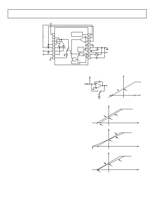
Figure 10. Bipolar Offset
SVFC CONNECTION FOR BIPOLAR INPUT VOLTAGES
A bipolar input voltage of ? V can be accommodated by
injecting a 250 礎 current into Pin 5 (see Figure 10). A 5 V
signal provides a zero sum current at the integrator summing
junction, which results in a zero-output frequency; a +5 V signal
provides a 0.5 mA (full-scale) sum current, which results in the
full-scale output frequency.
Using an external resistor to inject the offset current has some
effect on the bipolar offset temperature coefficient. The ideal
transfer curve with bipolar inputs is shown in Figure 11. The
user actually has four options to use in injecting the bipolar
offset current into the inverting input of the op amp:
1. Use an external resistor for ROS and the internal 20 k&
resistor for RIN (as shown in Figure 10).
2. Use the internal 20 k& resistor as R
OS
and an external R
IN
.
3. Use two external resistors.
4. Use two internal resistors for R
IN
and R
OS
(available on
PLCC version only).
Option 4 provides the closest to the ideal transfer function as
diagrammed in Figure 11. Figure 12 shows the effects of the
transfer relation on the other three options. In the first case, the
slope of the transfer function is unchanged with temperature.
However, V
ZERO
(the input voltage required to produce an output
frequency of 0 Hz) and F
ZERO
(the output frequency when
V
IN
= 0 V) changes as the transfer function is displaced parallel
to the voltage axis with temperature. In the second case, FZERO
remains constant, but VZERO changes as the transfer function
rotates about FZERO with temperature changes. In the third case,
with two external resistors, the VZERO point remains invariant
while the slope and offset of the transfer function change with
temperature. If selecting this third option, the user should select
low drift, matched resistors.
V
REF
IN
R
OS
R
IN
IDEAL
TRANSFER
RELATION
V
ZERO
F
OUT
F
ZERO
5V
+5V
V
IN
Figure 11. Ideal Bipolar Input Transfer Curve over Temperature
IDEAL
F
OUT
F
ZERO
V
IN
TEMPERATURE
PERTURBED
TRANSFER
V
ZERO
5V
CASE 1
R
IN
< INTERNAL
R
OS
< EXTERNAL
IDEAL
F
OUT
F
ZERO
V
IN
TEMPERATURE
PERTURBED
V
ZERO
5V
CASE 2
R
IN
< EXTERNAL
R
OS
< INTERNAL
IDEAL
F
OUT
F
ZERO
V
IN
TEMPERATURE
PERTURBED
V
ZERO
5V
CASE 3
R
IN
< EXTERNAL
R
OS
< EXTERNAL
Figure 12. Actual Bipolar Input Transfer over Temperature
相关PDF资料 |
PDF描述 |
|---|---|
| AD654JNZ/+ | IC CONV VOLT-FREQ 500KHZ 8DIP |
| AD7740YRM | IC CONVERTER V TO FREQ 8-MSOP |
| ADM1070ARTZ-REEL7 | IC CTRLR HOTSWAP -48V SOT23-6 |
| ADM1073ARU-REEL | IC CTRLR HOTSWAP -48V 14TSSOP |
| ADM4210-2AUJZ-RL7 | IC CTLR HOTSWAP LV TSOT23-6 |
相关代理商/技术参数 |
参数描述 |
|---|---|
| AD652SQ/883B | 功能描述:电压频率转换及频率电压转换 IC - SYNC V/F CONVERTER RoHS:否 制造商:Texas Instruments 全标度频率:4000 KHz 线性误差:+/- 1 % FSR 电源电压-最大: 电源电压-最小: 最大工作温度:+ 85 C 最小工作温度:- 25 C 安装风格:Through Hole 封装 / 箱体:PDIP-14 封装:Tube |
| AD652SQ/883B2 | 制造商:AD 制造商全称:Analog Devices 功能描述:Monolithic Synchronous Voltage-to-Frequency Converter |
| AD652SQ2 | 制造商:AD 制造商全称:Analog Devices 功能描述:Monolithic Synchronous Voltage-to-Frequency Converter |
| AD652SQ883B2 | 制造商:AD 制造商全称:Analog Devices 功能描述:Monolithic Synchronous Voltage-to-Frequency Converter |
| AD652SW | 制造商:AD 制造商全称:Analog Devices 功能描述:Monolithic Synchronous Voltage-to-Frequency Converter |
发布紧急采购,3分钟左右您将得到回复。