- 您现在的位置:买卖IC网 > Datasheet目录38 > AD652SQ (Analog Devices Inc)IC V-F CONV SYNCH MONO 5V 16CDIP Datasheet资料下载
参数资料
| 型号: | AD652SQ |
| 厂商: | Analog Devices Inc |
| 文件页数: | 18/28页 |
| 文件大小: | 779K |
| 描述: | IC V-F CONV SYNCH MONO 5V 16CDIP |
| 标准包装: | 1 |
| 类型: | 电压至频率 |
| 频率 - 最大: | 2MHz |
| 全量程: | ±25ppm/°C |
| 线性: | ±0.005% |
| 安装类型: | 通孔 |
| 封装/外壳: | 16-CDIP(0.300",7.62mm) |
| 供应商设备封装: | 16-CDIP |
| 包装: | 管件 |
第1页第2页第3页第4页第5页第6页第7页第8页第9页第10页第11页第12页第13页第14页第15页第16页第17页当前第18页第19页第20页第21页第22页第23页第24页第25页第26页第27页第28页
AD652
Rev. C | Page 18 of 28
This can be shown in equation form, where fC is the AD654
output frequency and fOUT is the AD652 output frequency:
V
10
MHz
1
1
C
V
f =
?/DIV>
?/DIV>
?/DIV>
?/DIV>
?/DIV>
?/DIV>
?/DIV>
?/DIV>
?/DIV>
?/DIV>
?/DIV>
?/DIV>
=
V
10
2
C
2
OUT
f
V
f
( )( )
?/DIV>
?/DIV>
?/DIV>
?/DIV>
?/DIV>
?/DIV>
?/DIV>
?/DIV>
=
V
10
V
10
2
MHz
1
2
1
OUT
V
V
f
f
OUT
= V
1
?V
2
?5 kHz/V
2
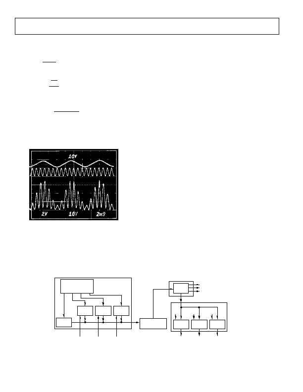
The scope photo in Figure 24 shows V
1
and V
2
(top two traces)
and the output of the F-V (bottom trace).
V
1
V
2
V
OUT
Figure 24. Multiplier Waveforms
SINGLE-LINE MULTIPLEXED DATA TRANSMISSION
It is often necessary to measure several different signals and
relay the information to some remote location using a mini-
mum amount of cable. Multiple AD652 SVFC devices may be
used with a multiphase clock to combine these measurements
for serial transmission and demultiplexing. Figure 25 shows a
block diagram of a single-line multiplexed data transmission
system with high noise immunity. Figure 26, Figure 27, and
Figure 30 show the SVFC multiplexer, a representative means of
data transmission, and an SVFC demultiplexer respectively.
Multiplexer
Figure 30 shows the SVFC multiplexer. The clock inputs for the
several SVFC channels are generated by a TIM9904A 4-phase
clock driver, and the frequency outputs are combined by
strapping all the frequency output pins together (a wire OR
connection). The one-shot in the AD652 sets the pulse width of
the frequency output pulses to be slightly shorter than one
quarter of the clock period. Synchronization is achieved by
applying one of the four available phases to a fixed TTL one-
shot (121) and combining the output with external transistor.
The width of this sync pulse is shorter than the width of the
frequency output pulses to facilitate decoding the signal. The
RC lag network on the input of the one-shot provides a slight
delay between the rising edge of the clock and the sync pulse in
order to match the 150 ns delay of the AD652 between the
rising edge of the clock and the output pulse.
Transmitter
The multiplex signal can be transmitted in any manner suitable
to the task at hand. A pulse transformer or an opto-isolator can
provide galvanic isolation; extremely high voltage isolation or
transmission through severe RF environments can be accomp-
lished with a fiber optic link; telemetry can be achieved with a
radio link. The circuit shown in Figure 27 uses an EIA RS-422
standard for digital data transmission over a balanced line.
Figure 24 shows the waveforms of the four clock phases and the
multiplex output signal. Note that the sync pulse is present
every clock cycle, but the data pulses are no more frequent than
every other clock cycle since the maximum output frequency
from the SVFC is half the clock frequency. The clock frequency
used in this circuit is 819.2 kHz, which provides more than
16 bits of resolution if 100 ms gate time is allowed for counting
pulses of the decoded output frequencies.
AD652
V
IN1
AD652
V
IN2
AD652
V
IN3
ONE
SHOT
?SPAN class="pst AD652SQ_2632819_6">1 ?SPAN class="pst AD652SQ_2632819_6">2 ?SPAN class="pst AD652SQ_2632819_6">3 ?SPAN class="pst AD652SQ_2632819_6">4
CLK
GENERATOR
SVFC MULTIPLEXER
(SEE FIGURE 26)
AD652
?/DIV>
2
V
OUT1
AD652
?/DIV>
3
V
OUT2
AD652
?/DIV>
4
V
OUT3
SVFC
DEMUX
f1
f2
f3
SVFC DEMULTIPLEXER
(SEE FIGURE 30)
DEMULTIPLEXER FREQUENCY TO
VOLTAGE CONVERSION
(SEE FIGURE 31)
TRANSMISSION
LINK
TRANSMISSION
LINK
(SEE FIGURE 27)
Figure 25. Single-Line Multiplexed Data Transmission Block Diagram
相关PDF资料 |
PDF描述 |
|---|---|
| AD654JNZ/+ | IC CONV VOLT-FREQ 500KHZ 8DIP |
| AD7740YRM | IC CONVERTER V TO FREQ 8-MSOP |
| ADM1070ARTZ-REEL7 | IC CTRLR HOTSWAP -48V SOT23-6 |
| ADM1073ARU-REEL | IC CTRLR HOTSWAP -48V 14TSSOP |
| ADM4210-2AUJZ-RL7 | IC CTLR HOTSWAP LV TSOT23-6 |
相关代理商/技术参数 |
参数描述 |
|---|---|
| AD652SQ/883B | 功能描述:电压频率转换及频率电压转换 IC - SYNC V/F CONVERTER RoHS:否 制造商:Texas Instruments 全标度频率:4000 KHz 线性误差:+/- 1 % FSR 电源电压-最大: 电源电压-最小: 最大工作温度:+ 85 C 最小工作温度:- 25 C 安装风格:Through Hole 封装 / 箱体:PDIP-14 封装:Tube |
| AD652SQ/883B2 | 制造商:AD 制造商全称:Analog Devices 功能描述:Monolithic Synchronous Voltage-to-Frequency Converter |
| AD652SQ2 | 制造商:AD 制造商全称:Analog Devices 功能描述:Monolithic Synchronous Voltage-to-Frequency Converter |
| AD652SQ883B2 | 制造商:AD 制造商全称:Analog Devices 功能描述:Monolithic Synchronous Voltage-to-Frequency Converter |
| AD652SW | 制造商:AD 制造商全称:Analog Devices 功能描述:Monolithic Synchronous Voltage-to-Frequency Converter |
发布紧急采购,3分钟左右您将得到回复。