- 您现在的位置:买卖IC网 > Datasheet目录38 > AD652SQ (Analog Devices Inc)IC V-F CONV SYNCH MONO 5V 16CDIP Datasheet资料下载
参数资料
| 型号: | AD652SQ |
| 厂商: | Analog Devices Inc |
| 文件页数: | 9/28页 |
| 文件大小: | 779K |
| 描述: | IC V-F CONV SYNCH MONO 5V 16CDIP |
| 标准包装: | 1 |
| 类型: | 电压至频率 |
| 频率 - 最大: | 2MHz |
| 全量程: | ±25ppm/°C |
| 线性: | ±0.005% |
| 安装类型: | 通孔 |
| 封装/外壳: | 16-CDIP(0.300",7.62mm) |
| 供应商设备封装: | 16-CDIP |
| 包装: | 管件 |
第1页第2页第3页第4页第5页第6页第7页第8页当前第9页第10页第11页第12页第13页第14页第15页第16页第17页第18页第19页第20页第21页第22页第23页第24页第25页第26页第27页第28页
AD652
Rev. C | Page 9 of 28
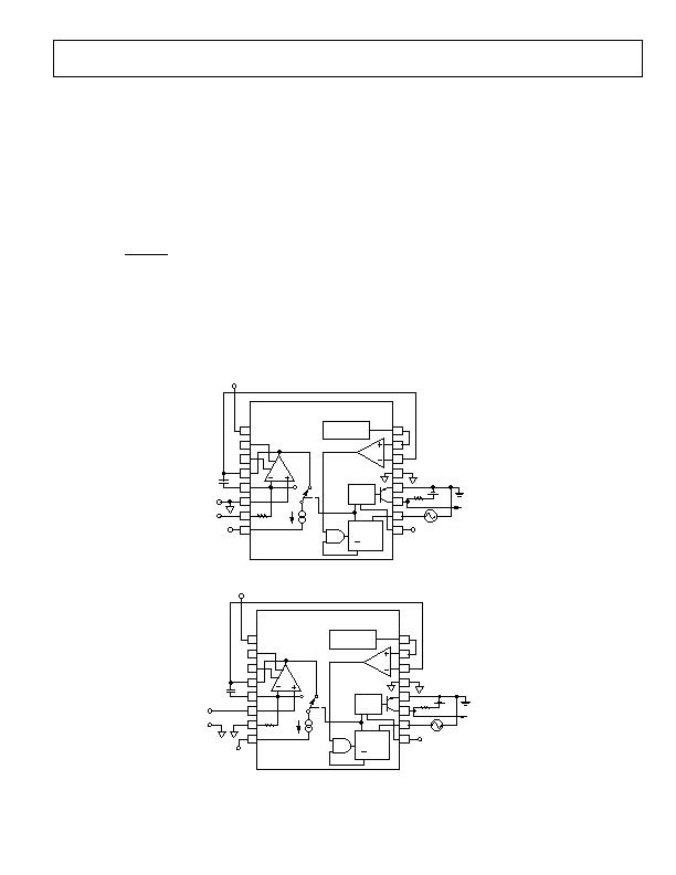
SVFC CONNECTION FOR DUAL SUPPLY, POSITIVE
INPUT VOLTAGES
Figure 8 shows the AD652 connection scheme for the
traditional dual supply, positive input mode of operation. The
盫
S
range is from ? V to ?8 V. When +V
S
is lower than 9.0 V,
As shown in Figure 8, three additional connections are required
The first connection is to short Pin 13 to Pin 8 (Analog Ground
to VS) and add a pull-up resistor to +VS (as shown in
Figure 21). The pull-up resistor is determined by the following
equation:
礎
500
V
5
2
=
S
PULLUP
V
R
These connections ensure proper operation of the 5 V reference.
Tie Pin 16 to Pin 6 (as shown in Figure 21) to ensure that the
integrator output ramps down far enough to trip the
comparator.
The CERDIP-packaged AD652 accepts either a 0 V to 10 V or
0 mA to 0.5 mA full-scale input signal. The temperature drift of
the AD652 is specified for a 0 V to 10 V input range using the
internal 20 k& resistor. If a current input is used, the gain drift is
degraded by a maximum of 100 ppm/癈 (the TC of the 20 k&
resistor). If an external resistor is connected to Pin 5 to establish
a different input voltage range, drift is induced to the extent that
the external resistors TC differs from the TC of the internal
resistor. The external resistor used to establish a different input
voltage range should be selected to provide a full-scale current
of 0.5 mA (i.e., 10 k& for 0 V to 5 V).
SVFC CONNECTIONS FOR NEGATIVE INPUT
VOLTAGES
Voltages that are negative with respect to ground may be used
as the input to the AD652 SVFC. In this case, Pin 7 is grounded
and the input voltage is applied to Pin 6 (see Figure 9). In this
mode, the input voltage can go as low as 4 V above V
S
. In this
configuration, the input is a high impedance, and only the
20 nA (typical) input bias current of the op amp must be
supplied by the input signal. This is contrasted with the more
usual positive input voltage configuration, which has a 20 k&
input impedance and requires 0.5 mA from the signal source.
+
S
1
2
3
4
+
5
6
7
+V
S
V
IN
8
16
15
14
13
12
11
10
9
ONE
SHOT
AND
"D"
FLOP
Q CK
D
Q
1mA
20k&
AD652
SYNCHRONOUS
VOLTAGE-TO-
FREQUENCY
CONVERTER
5V
REFERENCE
R
L
5V
CLOCK
ANALOG
GND
DIGITAL
GND
FREQ
OUT
INT
V
S
Figure 8. Standard V/F Connection for Positive Input Voltage with Dual Supply
+V
S
1
2
3
4
5
6
7
+V
S
V
S
8
16
15
14
13
12
11
10
9
ONE
SHOT
AND
"D"
FLOP
Q CK
D
Q
1mA
20k&
AD652
SYNCHRONOUS
VOLTAGE-TO-
FREQUENCY
CONVERTER
5V
REFERENCE
R
L
5V
CLOCK
ANALOG
GND
DIGITAL
GND
FREQ
OUT
C
INT
+
V
IN
Figure 9. Negative Voltage Input
相关PDF资料 |
PDF描述 |
|---|---|
| AD654JNZ/+ | IC CONV VOLT-FREQ 500KHZ 8DIP |
| AD7740YRM | IC CONVERTER V TO FREQ 8-MSOP |
| ADM1070ARTZ-REEL7 | IC CTRLR HOTSWAP -48V SOT23-6 |
| ADM1073ARU-REEL | IC CTRLR HOTSWAP -48V 14TSSOP |
| ADM4210-2AUJZ-RL7 | IC CTLR HOTSWAP LV TSOT23-6 |
相关代理商/技术参数 |
参数描述 |
|---|---|
| AD652SQ/883B | 功能描述:电压频率转换及频率电压转换 IC - SYNC V/F CONVERTER RoHS:否 制造商:Texas Instruments 全标度频率:4000 KHz 线性误差:+/- 1 % FSR 电源电压-最大: 电源电压-最小: 最大工作温度:+ 85 C 最小工作温度:- 25 C 安装风格:Through Hole 封装 / 箱体:PDIP-14 封装:Tube |
| AD652SQ/883B2 | 制造商:AD 制造商全称:Analog Devices 功能描述:Monolithic Synchronous Voltage-to-Frequency Converter |
| AD652SQ2 | 制造商:AD 制造商全称:Analog Devices 功能描述:Monolithic Synchronous Voltage-to-Frequency Converter |
| AD652SQ883B2 | 制造商:AD 制造商全称:Analog Devices 功能描述:Monolithic Synchronous Voltage-to-Frequency Converter |
| AD652SW | 制造商:AD 制造商全称:Analog Devices 功能描述:Monolithic Synchronous Voltage-to-Frequency Converter |
发布紧急采购,3分钟左右您将得到回复。