- 您现在的位置:买卖IC网 > Datasheet目录38 > AD652SQ (Analog Devices Inc)IC V-F CONV SYNCH MONO 5V 16CDIP Datasheet资料下载
参数资料
| 型号: | AD652SQ |
| 厂商: | Analog Devices Inc |
| 文件页数: | 11/28页 |
| 文件大小: | 779K |
| 描述: | IC V-F CONV SYNCH MONO 5V 16CDIP |
| 标准包装: | 1 |
| 类型: | 电压至频率 |
| 频率 - 最大: | 2MHz |
| 全量程: | ±25ppm/°C |
| 线性: | ±0.005% |
| 安装类型: | 通孔 |
| 封装/外壳: | 16-CDIP(0.300",7.62mm) |
| 供应商设备封装: | 16-CDIP |
| 包装: | 管件 |
第1页第2页第3页第4页第5页第6页第7页第8页第9页第10页当前第11页第12页第13页第14页第15页第16页第17页第18页第19页第20页第21页第22页第23页第24页第25页第26页第27页第28页
AD652
Rev. C | Page 11 of 28
NC = NO CONNECT
5
7
8
NC
V
IN
+
NC NC
6
9
10
AD652
SYNCHRONOUS
VOLTAGE-TO-
FREQUENCY
CONVERTER
10k&
10k&
16k&
4k&
A. PLCC 0V TO 10V INPUT
5
7
8
NC
NC
NC
6
9
10
AD652
SYNCHRONOUS
VOLTAGE-TO-
FREQUENCY
CONVERTER
10k&
10k&
16k&
4k&
B. PLCC 0V TO 8V INPUT
V
IN
+
5
7
8
NC
NC NC
6
9
10
AD652
SYNCHRONOUS
VOLTAGE-TO-
FREQUENCY
CONVERTER
10k&
10k&
16k&
4k&
C. PLCC 0V TO 5V INPUT
V
IN
+
5
7
8
NC
V
IN
?SPAN class="pst AD652SQ_2632819_4">5V
NC
6
9
10
AD652
SYNCHRONOUS
VOLTAGE-TO-
FREQUENCY
CONVERTER
10k&
10k&
16k&
4k&
D. PLCC?/SPAN>5V INPUT
5V REF
20
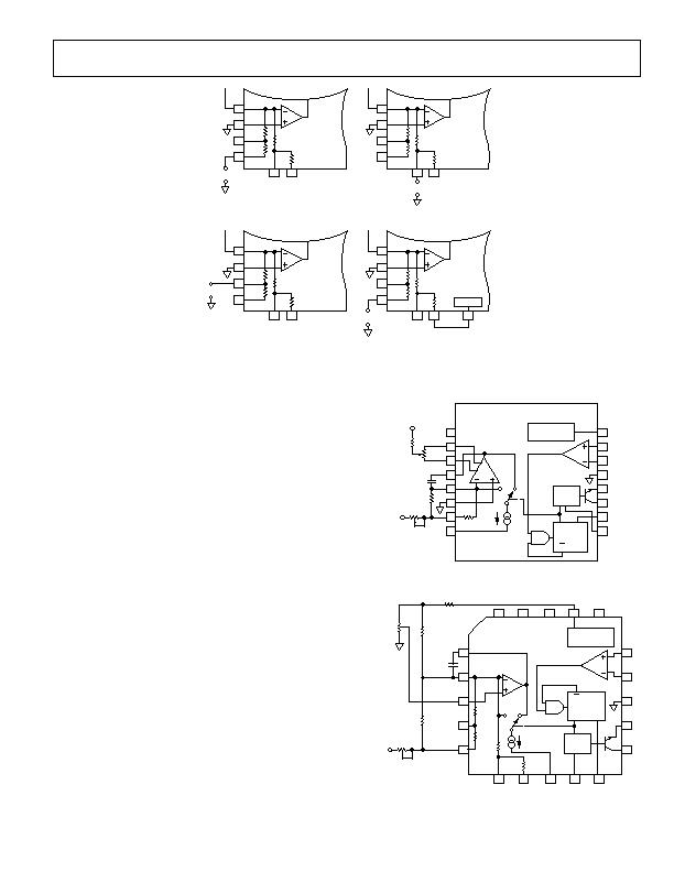
Figure 13.
PLCC CONNECTIONS
The PLCC packaged AD652 offers additional input resistors not
found on the CERDIP-packaged device. These resistors provide
the user with additional input voltage ranges. Besides the 10 V
range available using the on-chip resistor in the CERDIP the
PLCC also offers 8 V and 5 V ranges. Figure 13A to Figure 13C
show the proper connections for these ranges with positive
input voltages. For negative input voltages, the appropriate
resistor should be tied to analog ground and the input voltage
should be applied to Pin 6, the + input of the op amp.
Bipolar input voltages can be accommodated by injecting
250 礎 into Pin 5 with the use of the 5 V reference and the
input resistors. For the ? V or ?.5 V range, the reference
output, Pin 20, should be tied to Pin 10. The input signal should
then be applied to Pin 8 for a ? V signal and to Pin 7 for a
?.5 V signal. The input connections for a ? V range are
shown in Figure 13D. For a ? V range, the input signal should
be applied to Pin 9, and Pin 20 should be connected to Pin 8.
GAIN AND OFFSET CALIBRATION
The gain error of the AD652 is laser trimmed to within ?.5%.
If higher accuracy is required, the internal 20 k& resistor must
be shunted with a 2 M& resistor to produce a parallel equivalent
that is 1% lower in value than the nominal 20 k&. Full-scale
adjustment is then accomplished using a 500 & series trimmer.
See Figure 14 and Figure 15. When negative input voltages are
used, this 500 & trimmer is tied to ground and Pin 6 is the
input pin.
1
2
3
4
5
6
7
8
16
15
14
13
12
11
10
9
ONE
SHOT
AND
"D"
FLOP
Q CK
D
Q
1mA
20k&
AD652
SYNCHRONOUS
VOLTAGE-TO-
FREQUENCY
CONVERTER
5V
REFERENCE
V
IN
+V
S
0.02?/SPAN>F
2M&
500&
250k&
20k&
Figure 14. CERDIP Gain and Offset Trim
4
5
6
7
8
18
17
16
15
14
9
10
11
12
13
3
2
1
20
19
1mA
5V
REFERENCE
AD652
AND
"D"
FLOP
Q
CK
D
Q
ONE
SHOT
10k&
10k&
16k&
4k&
SYNCHRONOUS
VOLTAGE-TO-FREQUENCY
CONVERTER
V
IN
500&
500&
2M&
0.02?/SPAN>F
20k&
350k&
?SPAN class="pst AD652SQ_2632819_4">3.5mV
OFFSET
TRIM
Figure 15. PLCC Gain and Offset Trim
相关PDF资料 |
PDF描述 |
|---|---|
| AD654JNZ/+ | IC CONV VOLT-FREQ 500KHZ 8DIP |
| AD7740YRM | IC CONVERTER V TO FREQ 8-MSOP |
| ADM1070ARTZ-REEL7 | IC CTRLR HOTSWAP -48V SOT23-6 |
| ADM1073ARU-REEL | IC CTRLR HOTSWAP -48V 14TSSOP |
| ADM4210-2AUJZ-RL7 | IC CTLR HOTSWAP LV TSOT23-6 |
相关代理商/技术参数 |
参数描述 |
|---|---|
| AD652SQ/883B | 功能描述:电压频率转换及频率电压转换 IC - SYNC V/F CONVERTER RoHS:否 制造商:Texas Instruments 全标度频率:4000 KHz 线性误差:+/- 1 % FSR 电源电压-最大: 电源电压-最小: 最大工作温度:+ 85 C 最小工作温度:- 25 C 安装风格:Through Hole 封装 / 箱体:PDIP-14 封装:Tube |
| AD652SQ/883B2 | 制造商:AD 制造商全称:Analog Devices 功能描述:Monolithic Synchronous Voltage-to-Frequency Converter |
| AD652SQ2 | 制造商:AD 制造商全称:Analog Devices 功能描述:Monolithic Synchronous Voltage-to-Frequency Converter |
| AD652SQ883B2 | 制造商:AD 制造商全称:Analog Devices 功能描述:Monolithic Synchronous Voltage-to-Frequency Converter |
| AD652SW | 制造商:AD 制造商全称:Analog Devices 功能描述:Monolithic Synchronous Voltage-to-Frequency Converter |
发布紧急采购,3分钟左右您将得到回复。