- 您现在的位置:买卖IC网 > PDF目录373890 > AD6600ST (Analog Devices, Inc.) Dual Channel, Gain-Ranging ADC with RSSI PDF资料下载
参数资料
| 型号: | AD6600ST |
| 厂商: | Analog Devices, Inc. |
| 英文描述: | Dual Channel, Gain-Ranging ADC with RSSI |
| 中文描述: | 双通道,增益测距型ADC的RSSI |
| 文件页数: | 15/24页 |
| 文件大小: | 303K |
| 代理商: | AD6600ST |
REV. 0
AD6600
–15–
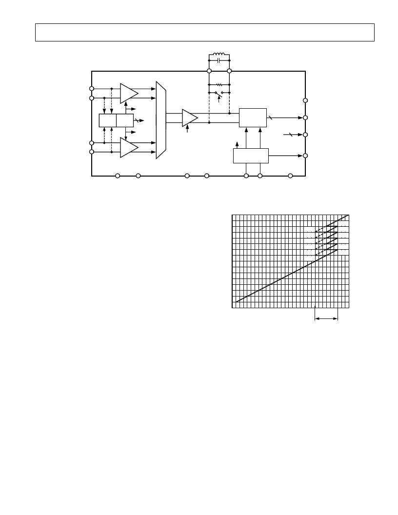
THEORY OF OPERATION
The AD6600, dual-channel, gain-ranging ADC integrates ana-
log IF circuitry with high speed data conversion. Each analog
input stage is a 1 GHz, 0 dB to
–
24 dB, phase-compensated step
attenuator; the step size in each attenuator is 12 dB. Both input
stages drive an analog multiplex function followed by a 12dB/
18 dB gain amplifier. A simple LC noise filter at the output of
the gain amplifier is required to resonate at the desired IF. This
resonant filter port precedes a wide input bandwidth (450 MHz)
track-and-hold followed by an 11-bit analog-to-digital converter
(ADC). A high speed synchronous peak detector monitors sig-
nal strength at both input channels. The peak detector drives
RSSI circuitry that automatically adjusts attenuation and gain
on a clock-by-clock basis. The three RSSI indicator bits and the
eleven ADC bits are available at the output providing an exponent
and mantissa data format. Together these integrated components
form an IF sampling, high dynamic range ADC system.
It is helpful to view this device as a stand-alone ADC using
automatic gain control. The gain control referred to in this data
sheet as
“
gain-ranging
”
works to maintain a constant SNR over
as wide a range as possible.
As stated previously, the AD6600 has a floating-point output:
eleven mantissa bits and three exponent bits. As shown in Fig-
ure 16, at the lowest input levels SNR increases 1 dB for a 1 dB
increase in input power. In this range, the AD6600 is set for
maximum gain. However, when the input signal level reaches
the gain-ranging section (approximately
–
42 dBFS), the SNR is
contained between about 50 dB and 56 dB or between 44 dB and
56 dB including the effects of hysteresis. Although Figure 16
does not indicate so, there are slight differences between the
SNR from one gain range to the next as the gain amp switches
between 12 dB and 18 dB. Once the final RSSI range has been
exceeded (approximately
–
12 dBFS), SNR again increases 1 dB
per 1 dB input power increase until converter full scale is reached.
Again, this performance is very much like the effects of a typical
analog AGC loop.
GAIN
A/D
CONVERTER
TIMING
ENCODE
SELECT GAIN
+12, +18dB
ENCODE
FLT
FLT
NOISE FILTER
RESONANT
PORT
630
RSSI
3
TWO'S
COMPLEMENT
11
AB_OUT
D10
–
D0
RSSI [2:0]
CLK2
DVCC
ENC
ENC
GND
AVCC
B_SEL
A_SEL
A
GAIN
GAIN
RSSI
3
0dB,
–
12dB,
–
24dB
ATTEN
ATTEN
0dB,
–
12dB,
–
24dB
DETECT
PEAK
SET
RSSI
AIN
AIN
BIN
BIN
AD6600
Figure 15. Functional Block Diagram
SNR
–
dB
–
12
–
18
–
24
–
48
–
54
–
60
–
66
–
72
–
78
–
84
–
90
–
96
24 28
A
–
32 36 40 44 48 52 56 60
–
42
–
30
–
36
0
–
90
20
16
12
8
4
0
12dB SNR WINDOW
101
100
011
010
001
000
101
100
011
010
001
000
Figure 16. SNR for Gain-Ranging ADC
AD6600 SUBCIRCUITS
Input Step Attenuator and Gain Stage
The AD6600 has two identical input attenuators, Channel A
and Channel B. These dual inputs are typically used as diversity
channels but may also process two independent IF signals. For
maximum oversampling the device is used in single channel mode;
in this case only one input channel is required. The attenuator
steps are 0 dB,
–
12 dB and
–
24 dB. The attenuator settings are
based on the decisions of the RSSI stage (see Peak Detector/
RSSI section). The outputs of the attenuators connect to an
analog multiplexer that selects either Channel A or B for subse-
quent processing (see Input Mode). The selected signal drives
a dual-gain amplifier set to either 12 dB or 18 dB; the selected
gain is also determined by the RSSI stage. Therefore, based on
all possible combinations of attenuation and gain, the input
signal receives
–
12 dB to +18 dB of voltage gain in 6 dB steps
(Table I). Overall gain-matching is typically within 0.1 dB. With
a bandwidth of 1 GHz, the phase delay through the front-end
ranges from 0.2 degrees to 0.5 degrees, depending on input
frequency. Additionally, the input impedance does not change
with attenuator settings so there is no AM-to-PM distortion.
相关PDF资料 |
PDF描述 |
|---|---|
| AD660AN | Monolithic 16-Bit Serial/Byte DACPORT |
| AD660AR | Monolithic 16-Bit Serial/Byte DACPORT |
| AD660BN | Monolithic 16-Bit Serial/Byte DACPORT |
| AD660BR | Monolithic 16-Bit Serial/Byte DACPORT |
| AD660SQ | Monolithic 16-Bit Serial/Byte DACPORT |
相关代理商/技术参数 |
参数描述 |
|---|---|
| AD6600ST/PCB | 制造商:Analog Devices 功能描述:Evaluation Board For Dual Channel, Gain-Ranging ADC With RSSI 制造商:Analog Devices 功能描述:DUAL CH, GAIN-RANGING ADC W/ RSSI - Bulk |
| AD660AN | 功能描述:IC DAC 16BIT MONO W/VREF 24-DIP RoHS:否 类别:集成电路 (IC) >> 数据采集 - 数模转换器 系列:DACPORT® 产品培训模块:Data Converter Fundamentals DAC Architectures 标准包装:750 系列:- 设置时间:7µs 位数:16 数据接口:并联 转换器数目:1 电压电源:双 ± 功率耗散(最大):100mW 工作温度:0°C ~ 70°C 安装类型:表面贴装 封装/外壳:28-LCC(J 形引线) 供应商设备封装:28-PLCC(11.51x11.51) 包装:带卷 (TR) 输出数目和类型:1 电压,单极;1 电压,双极 采样率(每秒):143k |
| AD660ANZ | 功能描述:IC DAC 16BIT MONO W/VREF 24-DIP RoHS:是 类别:集成电路 (IC) >> 数据采集 - 数模转换器 系列:DACPORT® 标准包装:1 系列:- 设置时间:4.5µs 位数:12 数据接口:串行,SPI? 转换器数目:1 电压电源:单电源 功率耗散(最大):- 工作温度:-40°C ~ 125°C 安装类型:表面贴装 封装/外壳:8-SOIC(0.154",3.90mm 宽) 供应商设备封装:8-SOICN 包装:剪切带 (CT) 输出数目和类型:1 电压,单极;1 电压,双极 采样率(每秒):* 其它名称:MCP4921T-E/SNCTMCP4921T-E/SNRCTMCP4921T-E/SNRCT-ND |
| AD660ANZ1 | 制造商:AD 制造商全称:Analog Devices 功能描述:Monolithic 16-Bit Serial/Byte DACPORT |
| AD660AR | 功能描述:IC DAC 16BIT MONO W/VREF 24-SOIC RoHS:否 类别:集成电路 (IC) >> 数据采集 - 数模转换器 系列:DACPORT® 产品培训模块:Data Converter Fundamentals DAC Architectures 标准包装:750 系列:- 设置时间:7µs 位数:16 数据接口:并联 转换器数目:1 电压电源:双 ± 功率耗散(最大):100mW 工作温度:0°C ~ 70°C 安装类型:表面贴装 封装/外壳:28-LCC(J 形引线) 供应商设备封装:28-PLCC(11.51x11.51) 包装:带卷 (TR) 输出数目和类型:1 电压,单极;1 电压,双极 采样率(每秒):143k |
发布紧急采购,3分钟左右您将得到回复。