- 您现在的位置:买卖IC网 > PDF目录373890 > AD6620PCB (Analog Devices, Inc.) 65 MSPS Digital Receive Signal Processor PDF资料下载
参数资料
| 型号: | AD6620PCB |
| 厂商: | Analog Devices, Inc. |
| 英文描述: | 65 MSPS Digital Receive Signal Processor |
| 中文描述: | 65 MSPS的数字接收信号处理器 |
| 文件页数: | 21/43页 |
| 文件大小: | 354K |
| 代理商: | AD6620PCB |
第1页第2页第3页第4页第5页第6页第7页第8页第9页第10页第11页第12页第13页第14页第15页第16页第17页第18页第19页第20页当前第21页第22页第23页第24页第25页第26页第27页第28页第29页第30页第31页第32页第33页第34页第35页第36页第37页第38页第39页第40页第41页第42页第43页
AD6620
–21–
REV. 0
Amplitude Dither
The second dither option is Amplitude Dither or “Complex
Dither.” Amplitude Dither is enabled by setting Bit 2 of the
NCO Control Register at address 0x301 high. Amplitude Dither
improves performance by randomizing the amplitude quantiza-
tion errors within the angular to Cartesian conversion of the
NCO. This dither will be particularly useful when the NCO
frequency is close to an integer submultiple of the Input Data
Rate. However, this option may reduce spurs at the expense of a
slightly raised noise floor. Amplitude Dither and Phase Dither
can be used together, separately or not at all.
Phase Offset
The phase offset register adds an offset to the phase accumula-
tor of the NCO. This is a 16-bit register and is interpreted as a
16-bit unsigned integer. A 0 in this register corresponds to a 0
Radian offset and an FFFF hex corresponds to an offset of 2
π
(1 – 1/(2^16)) Radians. This register can be used to allow mul-
tiple AD6620s whose NCOs are synchronized to produce sine
waves with a known and steady phase difference.
NCO Synchronization
In order to achieve phase coherence between several AD6620s,
a SYNC_NCO pin is provided. When the internal register bit,
SYNC_M/S (Bit 3 of internal register 0x300), is set high,
SYNC_NCO provides a synchronization pulse on the rising
edge of CLK. When the SYNC_M/S bit is low, SYNC_NCO
accepts an external synchronization signal sampled on the rising
edge of CLK. When the AD6620 is a slave, the SYNC_NCO
signal need not be a short pulse. It may be taken high and held
for more than a CLK cycle in which case the NCO will be held
inactive until this pin is again lowered. If the device is run as a
sync slave in Single Channel Mode, the SYNC_NCO pin must
be held low for one sample period, usually one clock cycle. If the
device is run in Diversity Channel Real mode, the SYNC_NCO
must be high for two sample periods (clock cycles). In a system
with an array of AD6620s it is not necessary to use one as a
master. It may be desirable to generate a synchronization signal
elsewhere in the system and use that to control the AD6620. An
example of this may be in systems that receive packets of data.
In this case, the NCO my be resynchronized prior to the begin-
ning of the packet, thus giving a consistent phase relationship on
each burst. This allows for ease of use in a large system where
many AD6620s need be synchronized accurately across a large
backplane or installation.
The frequency of the SYNC_NCO pulses, and therefore the
accuracy of the synchronization, is determined by the value of
the NCO Sync Control Register at address 302 hex. The value
in this register is the SYNC_MASK and is interpreted as a
32-bit unsigned integer. This value controls the window around
the zero crossing of the NCO output sine wave in which the
NCO will output a SYNC_NCO pulse as a master. As a slave,
the value in this register will determine the number of MSBs
of the output sine wave that are synchronized with the master.
The Master and all slaves should use the same SYNC_MASK
word. This value should almost always be written as all 1s
(FFFFFFFF hex).
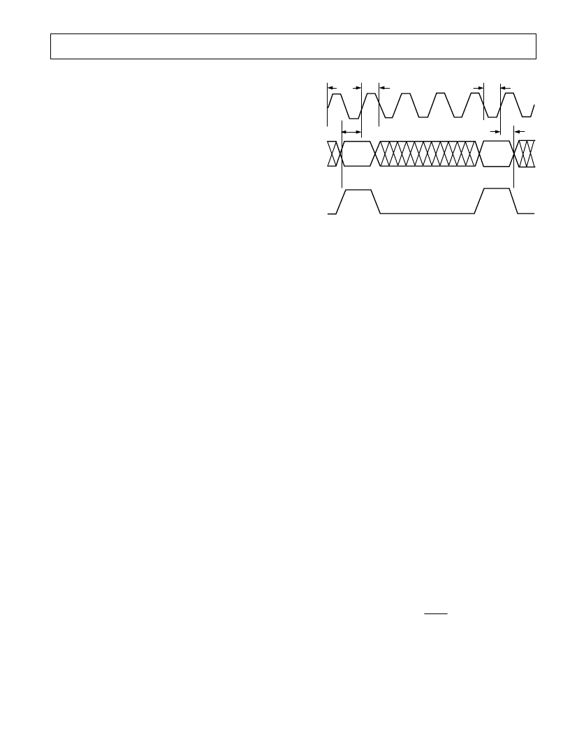
CLK
t
CHP
t
CPL
t
CS
t
CH
IN[15:0]
E[2:0]
A/B
N+1
N
t
CLK
Figure 39. SYNC_NCO Pin
Effects of A/B Input on the NCO
If the AD6620 is run in Single Channel Real mode using frac-
tional rate input timing, the A/B input is used to enable the
NCO advancement. If the A/B line is held high longer than one
clock period, the NCO will advance for each rising edge of the
CLK while A/B is high. This is not normally the desired result
and thus A/B must be taken low after the first CLK period to
prevent anomalous NCO results. See additional details under
Fractional Rate Timing.
Phase Continuous Tuning with the AD6620
For synchronization purposes, the AD6620 NCO phase is reset
each time the NCO frequency register is either written to or
read from. This is accomplished by forcing an NCO Sync to
occur. Normally, phase-continuous tuning is required on the
transmit path to control spectral leakage. On the receive path
this in not usually a constraint. However, if phase-continuous
tuning is required with the AD6620, it can be accomplished by
configuring the AD6620 as a Sync Slave. In this manner, no
internal NCO sync is generated when the NCO frequency regis-
ter is written to. If multiple AD6620s are synchronized together,
a common external sync pulse can be used to lock each of the
receivers together at the appropriate point in time. It is also
possible to reconfigure the AD6620 after the NCO frequency
register has been written so that the chip is once again a Sync
Master. The next time the NCO phase cycles through 0 degrees,
the NCO sync is exerted and the chip is again synchronized.
2ND ORDER CASCADED INTEGRATOR COMB FILTER
The CIC2 filter is a fixed-coefficient, decimating filter. It is
constructed as a second order CIC filter whose characteristics
are defined only by the decimation rate chosen. This filter can
process signals at the full rate of the input port (65 MHz) in all
input modes. The output rate of this stage is given by the equa-
tion below.
f
f
M
SAMP
SAMP
CIC
2
2
=
相关PDF资料 |
PDF描述 |
|---|---|
| AD6620AS | 65 MSPS Digital Receive Signal Processor |
| AD6620S | 65 MSPS Digital Receive Signal Processor |
| AD6620 | 65 MSPS Digital Receive Signal Processor(采样速率65MSPS的数字接收信号处理器) |
| AD6622AS | Four-Channel, 75 MSPS Digital Transmit Signal Processor TSP |
| AD6622PCB | Four-Channel, 75 MSPS Digital Transmit Signal Processor TSP |
相关代理商/技术参数 |
参数描述 |
|---|---|
| AD6620S | 制造商:AD 制造商全称:Analog Devices 功能描述:65 MSPS Digital Receive Signal Processor |
| AD6620S/PCB | 制造商:Analog Devices 功能描述:DUAL CHANNEL DECIMATING RECEIV 制造商:Analog Devices 功能描述:SGNL PROCESSOR 169CSPBGA - Bulk |
| AD6622 | 制造商:AD 制造商全称:Analog Devices 功能描述:Four-Channel, 75 MSPS Digital Transmit Signal Processor TSP |
| AD6622AS | 制造商:Analog Devices 功能描述:Transmit Signal Processor 128-Pin MQFP 制造商:Rochester Electronics LLC 功能描述:4 CHANNEL 65 MSPS DIGITAL UPCONVERTER - Bulk |
| AD6622PCB | 制造商:AD 制造商全称:Analog Devices 功能描述:Four-Channel, 75 MSPS Digital Transmit Signal Processor TSP |
发布紧急采购,3分钟左右您将得到回复。