- 您现在的位置:买卖IC网 > PDF目录373890 > AD6620PCB (Analog Devices, Inc.) 65 MSPS Digital Receive Signal Processor PDF资料下载
参数资料
| 型号: | AD6620PCB |
| 厂商: | Analog Devices, Inc. |
| 英文描述: | 65 MSPS Digital Receive Signal Processor |
| 中文描述: | 65 MSPS的数字接收信号处理器 |
| 文件页数: | 40/43页 |
| 文件大小: | 354K |
| 代理商: | AD6620PCB |
第1页第2页第3页第4页第5页第6页第7页第8页第9页第10页第11页第12页第13页第14页第15页第16页第17页第18页第19页第20页第21页第22页第23页第24页第25页第26页第27页第28页第29页第30页第31页第32页第33页第34页第35页第36页第37页第38页第39页当前第40页第41页第42页第43页
AD6620
–40–
REV. 0
/*—————————————————————————————*/
/*—————————————————————————————*/
spr1_asserted: /* SPORT1 Receive interrupt - do the fm demod and
increment the counter */
push sts;
/* Push the status stack */
/* Use secondary set of DAGs and Register file */
bit set mode1 SRD1H | SRD1L | SRD2H | SRD2L | SRRFH |
SRRFL;
nop;
/* Insert code here for processing I and Q data pairs. The DSP serial
port handler has placed the samples in fm_demod_data through
fm_demod_data+3 */
pop sts;
rti (db);
/* Pop the status stack */
/* Switch back to primary set of DAGs and Register file */
bit clr mode1 SRD1H | SRD1L | SRD2H | SRD2L | SRRFH |
SRRFL;
nop;
.ENDSEG;
/*—————————————————————————————*/
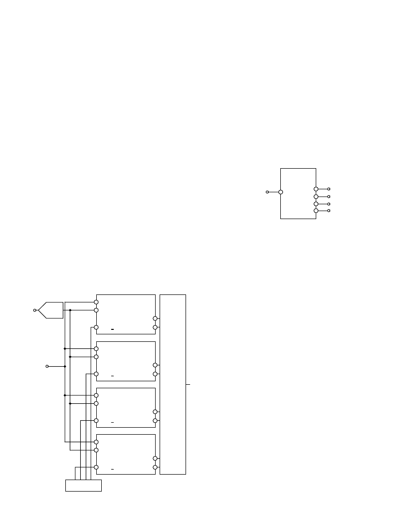
PARALLEL PROCESSING USING AD6620
If a single AD6620 does not have enough time to compute an
adequate filter, multiple AD6620s can be operated in parallel as
shown in Figure 57. In this example, the processing is distrib-
uted between four chips so that each chip can process more
taps. The outputs are then combined such that the desired data
rate is achieved.
AIN
ENCODE
CLOCK
AD6620 #1
CLK
D
IN
SYNC RCF
D
OUT
DV
OUT
AD6640
AD6620 #2
CLK
D
IN
SYNC RCF
D
OUT
DV
OUT
AD6620 #3
CLK
D
IN
SYNC RCF
D
OUT
DV
OUT
AD6620 #4
CLK
D
IN
SYNC RCF
D
OUT
DV
OUT
OUTPUT
SELECTOR
RCF TIMING
CONTROL
Figure 57. Parallel processing with the AD6620
In this application, one high speed ADC can feed parallel
AD6620s. Although not shown in this diagram, the SYNC_NCO
and SYNC_CICs are tied together and synchronized from an
external source with all chips run as SYNC_Slaves.
This architecture allows for each AD6620 to process four times
as many taps as would otherwise be possible. Consider the ex-
ample of an ADC clocked at 58.9824 MHz and a desired output
data rate of 4.9152 MHz. If a single AD6620 were used, the
decimation rate would be 12 (58.9824/4.9152) allowing for only
12 taps in the FIR filter. Not nearly enough for a usable digital
filter. Now consider the case where each AD6620 only provides
an output for one in four samples. In this case, the decimation
rate per chip would be four times larger, 48 in this example.
With a decimation of 48, more taps for the filter can be gener-
ated and produce a much better filter.
COUNTER
0 TO 47
CLOCK IN
COUNT = 0
COUNT = 11
COUNT = 23
COUNT = 35
Figure 58. RCF Timing Generator for Parallel Processing
Implementation of such a procedure is quite simple and basi-
cally shown in Figure 58. The filter design would proceed by
designing the filter to have the desired spectral characteristics
at its output rate. For our example here, each AD6620 would
have an output rate of 1.2288 MHz. The filter should be de-
signed such that the required rejection is attained directly at this
rate. This one filter is loaded into each chip. Upsampling is
achieved on the output by multiplexing between the different
AD6620 outputs which are staggered, in this case by 90 degrees
of the output data rate. Therefore, since the decimation rate
is 48 and four AD6620s are used, every 12 high speed clock
cycles a new AD6620 output should be selected. The most
direct method is to use these pulses to trigger the SYNC_RCF
signals. This staggering is required to properly phase the AD6620’s
internal computations. Once the chips have been synchronized
in this manner, they will begin producing DV
OUT
signals that
can be used to instruct the Output Selector which output is
valid.
The RCF Timing Control is responsible for proper phasing of
the AD6620s in the system. The example shown here is for the
example of four devices in parallel. It can easily be expanded to
any number of devices with this methodology. Since the AD6620s
are decimating by 48, the complete cycle time is 48 system
clocks. Thus the timing control must run modulo 48. When the
count is 0, the first RCF should be reset with a pulse that is one
clock cycle wide. Likewise, when the count is 11, 23 and 35,
RCF2, RCF3 and RCF4 should be reset respectively. This will
properly phase the AD6620s to run 90 degrees out of phase. If
this example consisted of six AD6620s, then they should be
reset on count 0, 7, 15, 23, 31 and 39. Following this method,
any number of AD6620s can be paralleled for higher data rates.
Once the AD6620 RCFs are properly phased, the DV
OUT
sig-
nals will then enable the output selector to know which outputs
should be connected at the correct point in time. In review, the
DV
OUT
signal pulses high when the RCF data is being placed on
相关PDF资料 |
PDF描述 |
|---|---|
| AD6620AS | 65 MSPS Digital Receive Signal Processor |
| AD6620S | 65 MSPS Digital Receive Signal Processor |
| AD6620 | 65 MSPS Digital Receive Signal Processor(采样速率65MSPS的数字接收信号处理器) |
| AD6622AS | Four-Channel, 75 MSPS Digital Transmit Signal Processor TSP |
| AD6622PCB | Four-Channel, 75 MSPS Digital Transmit Signal Processor TSP |
相关代理商/技术参数 |
参数描述 |
|---|---|
| AD6620S | 制造商:AD 制造商全称:Analog Devices 功能描述:65 MSPS Digital Receive Signal Processor |
| AD6620S/PCB | 制造商:Analog Devices 功能描述:DUAL CHANNEL DECIMATING RECEIV 制造商:Analog Devices 功能描述:SGNL PROCESSOR 169CSPBGA - Bulk |
| AD6622 | 制造商:AD 制造商全称:Analog Devices 功能描述:Four-Channel, 75 MSPS Digital Transmit Signal Processor TSP |
| AD6622AS | 制造商:Analog Devices 功能描述:Transmit Signal Processor 128-Pin MQFP 制造商:Rochester Electronics LLC 功能描述:4 CHANNEL 65 MSPS DIGITAL UPCONVERTER - Bulk |
| AD6622PCB | 制造商:AD 制造商全称:Analog Devices 功能描述:Four-Channel, 75 MSPS Digital Transmit Signal Processor TSP |
发布紧急采购,3分钟左右您将得到回复。