- 您现在的位置:买卖IC网 > PDF目录10532 > AD670JNZ (Analog Devices Inc)IC ADC 8BIT SGNL COND 20-DIP PDF资料下载
参数资料
| 型号: | AD670JNZ |
| 厂商: | Analog Devices Inc |
| 文件页数: | 1/12页 |
| 文件大小: | 0K |
| 描述: | IC ADC 8BIT SGNL COND 20-DIP |
| 标准包装: | 18 |
| 位数: | 8 |
| 采样率(每秒): | 10k |
| 数据接口: | 并联 |
| 转换器数目: | 1 |
| 功率耗散(最大): | 450mW |
| 电压电源: | 单电源 |
| 工作温度: | 0°C ~ 70°C |
| 安装类型: | 通孔 |
| 封装/外壳: | 20-DIP(0.300",7.62mm) |
| 供应商设备封装: | 20-PDIP |
| 包装: | 管件 |
| 输入数目和类型: | 1 个差分,单极;1 个差分,双极 |
| 产品目录页面: | 777 (CN2011-ZH PDF) |
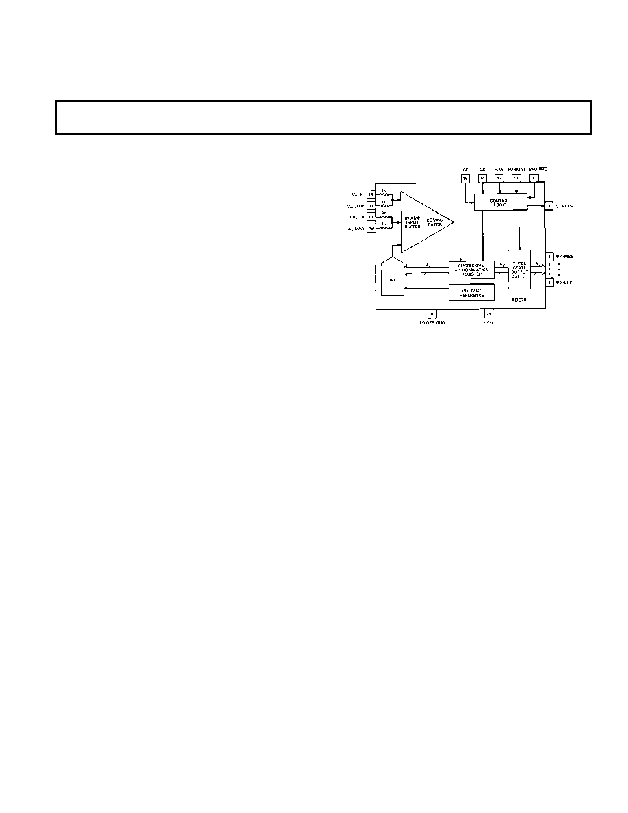
FUNCTIONAL BLOCK DIAGRAM
REV. A
Information furnished by Analog Devices is believed to be accurate and
reliable. However, no responsibility is assumed by Analog Devices for its
use, nor for any infringements of patents or other rights of third parties
which may result from its use. No license is granted by implication or
otherwise under any patent or patent rights of Analog Devices.
a
Low Cost Signal
Conditioning 8-Bit ADC
AD670
FEATURES
Complete 8-Bit Signal Conditioning A/D Converter
Including Instrumentation Amp and Reference
Microprocessor Bus Interface
10
s Conversion Speed
Flexible Input Stage: Instrumentation Amp Front End
Provides Differential Inputs and High Common-Mode
Rejection
No User Trims Required
No Missing Codes Over Temperature
Single +5 V Supply Operation
Convenient Input Ranges
20-Pin DIP or Surface-Mount Package
Low Cost Monolithic Construction
MIL-STD-883B Compliant Versions Available
GENERAL DESCRIPTION
The AD670 is a complete 8-bit signal conditioning analog-
to-digital converter. It consists of an instrumentation amplifier
front end along with a DAC, comparator, successive approxima-
tion register (SAR), precision voltage reference, and a three-
state output buffer on a single monolithic chip. No external
components or user trims are required to interface, with full
accuracy, an analog system to an 8-bit data bus. The AD670
will operate on the +5 V system supply. The input stage pro-
vides differential inputs with excellent common-mode rejection
and allows direct interface to a variety of transducers.
The device is configured with input scaling resistors to permit
two input ranges: 0 mV to 255 mV (1 mV/LSB) and 0 to 2.55 V
(10 mV/LSB). The AD670 can be configured for both unipolar
and bipolar inputs over these ranges. The differential inputs and
common-mode rejection of this front end are useful in applica-
tions such as conversion of transducer signals superimposed on
common-mode voltages.
The AD670 incorporates advanced circuit design and proven
processing technology. The successive approximation function
is implemented with I
2L (integrated injection logic). Thin-film
SiCr resistors provide the stability required to prevent missing
codes over the entire operating temperature range while laser
wafer trimming of the resistor ladder permits calibration of the
device to within
±1 LSB. Thus, no user trims for gain or offset
are required. Conversion time of the device is 10
s.
The AD670 is available in four package types and five grades.
The J and K grades are specified over 0
°C to +70°C and come
in 20-pin plastic DIP packages or 20-terminal PLCC packages.
The A and B grades (–40
°C to +85°C) and the S grade (–55°C
to +125
°C) come in 20-pin ceramic DIP packages.
One Technology Way, P.O. Box 9106, Norwood, MA 02062-9106, U.S.A.
Tel: 617/329-4700
Fax: 617/326-8703
The S grade is also available with optional processing to
MIL-STD-883 in 20-pin ceramic DIP or 20-terminal LCC
packages. The Analog Devices Military Products Databook
should be consulted for detailed specifications.
PRODUCT HIGHLIGHTS
1. The AD670 is a complete 8-bit A/D including three-state
outputs and microprocessor control for direct connection to
8-bit data buses. No external components are required to
perform a conversion.
2. The flexible input stage features a differential instrumenta-
tion amp input with excellent common-mode rejection. This
allows direct interface to a variety of transducers without
preamplification.
3. No user trims are required for 8-bit accurate performance.
4. Operation from a single +5 V supply allows the AD670 to
run off of the microprocessor’s supply.
5. Four convenient input ranges (two unipolar and two bipolar)
are available through internal scaling resistors: 0 mV to
255 mV (1 mV/LSB) and 0 V to 2.55 V (10 mV/LSB).
6. Software control of the output mode is provided. The user
can easily select unipolar or bipolar inputs and binary or 2s
complement output codes.
相关PDF资料 |
PDF描述 |
|---|---|
| VE-J4W-MY-F3 | CONVERTER MOD DC/DC 5.5V 50W |
| VI-B4V-MX-F2 | CONVERTER MOD DC/DC 5.8V 75W |
| LTC2291CUP#PBF | IC ADC DUAL 12BIT 25MSPS 64QFN |
| VI-B4V-MX-F1 | CONVERTER MOD DC/DC 5.8V 75W |
| VE-J4V-MY-F2 | CONVERTER MOD DC/DC 5.8V 50W |
相关代理商/技术参数 |
参数描述 |
|---|---|
| AD670JNZ | 制造商:Analog Devices 功能描述:IC 8-BIT ADC |
| AD670JP | 功能描述:IC ADC 8BIT SGNL COND 20-PLCC RoHS:否 类别:集成电路 (IC) >> 数据采集 - 模数转换器 系列:- 产品培训模块:Lead (SnPb) Finish for COTS Obsolescence Mitigation Program 标准包装:2,500 系列:- 位数:12 采样率(每秒):3M 数据接口:- 转换器数目:- 功率耗散(最大):- 电压电源:- 工作温度:- 安装类型:表面贴装 封装/外壳:SOT-23-6 供应商设备封装:SOT-23-6 包装:带卷 (TR) 输入数目和类型:- |
| AD670JP-REEL | 制造商:Analog Devices 功能描述:ADC Single SAR 8-bit Parallel 20-Pin PLCC T/R |
| AD670JP-REEL7 | 制造商:Analog Devices 功能描述: |
| AD670JPZ | 功能描述:IC ADC 8BIT SIGNAL COND 20-PLCC RoHS:是 类别:集成电路 (IC) >> 数据采集 - 模数转换器 系列:- 标准包装:1 系列:- 位数:14 采样率(每秒):83k 数据接口:串行,并联 转换器数目:1 功率耗散(最大):95mW 电压电源:双 ± 工作温度:0°C ~ 70°C 安装类型:通孔 封装/外壳:28-DIP(0.600",15.24mm) 供应商设备封装:28-PDIP 包装:管件 输入数目和类型:1 个单端,双极 |
发布紧急采购,3分钟左右您将得到回复。