- 您现在的位置:买卖IC网 > PDF目录10532 > AD670JNZ (Analog Devices Inc)IC ADC 8BIT SGNL COND 20-DIP PDF资料下载
参数资料
| 型号: | AD670JNZ |
| 厂商: | Analog Devices Inc |
| 文件页数: | 2/12页 |
| 文件大小: | 0K |
| 描述: | IC ADC 8BIT SGNL COND 20-DIP |
| 标准包装: | 18 |
| 位数: | 8 |
| 采样率(每秒): | 10k |
| 数据接口: | 并联 |
| 转换器数目: | 1 |
| 功率耗散(最大): | 450mW |
| 电压电源: | 单电源 |
| 工作温度: | 0°C ~ 70°C |
| 安装类型: | 通孔 |
| 封装/外壳: | 20-DIP(0.300",7.62mm) |
| 供应商设备封装: | 20-PDIP |
| 包装: | 管件 |
| 输入数目和类型: | 1 个差分,单极;1 个差分,双极 |
| 产品目录页面: | 777 (CN2011-ZH PDF) |
AD670
REV. A
–10–
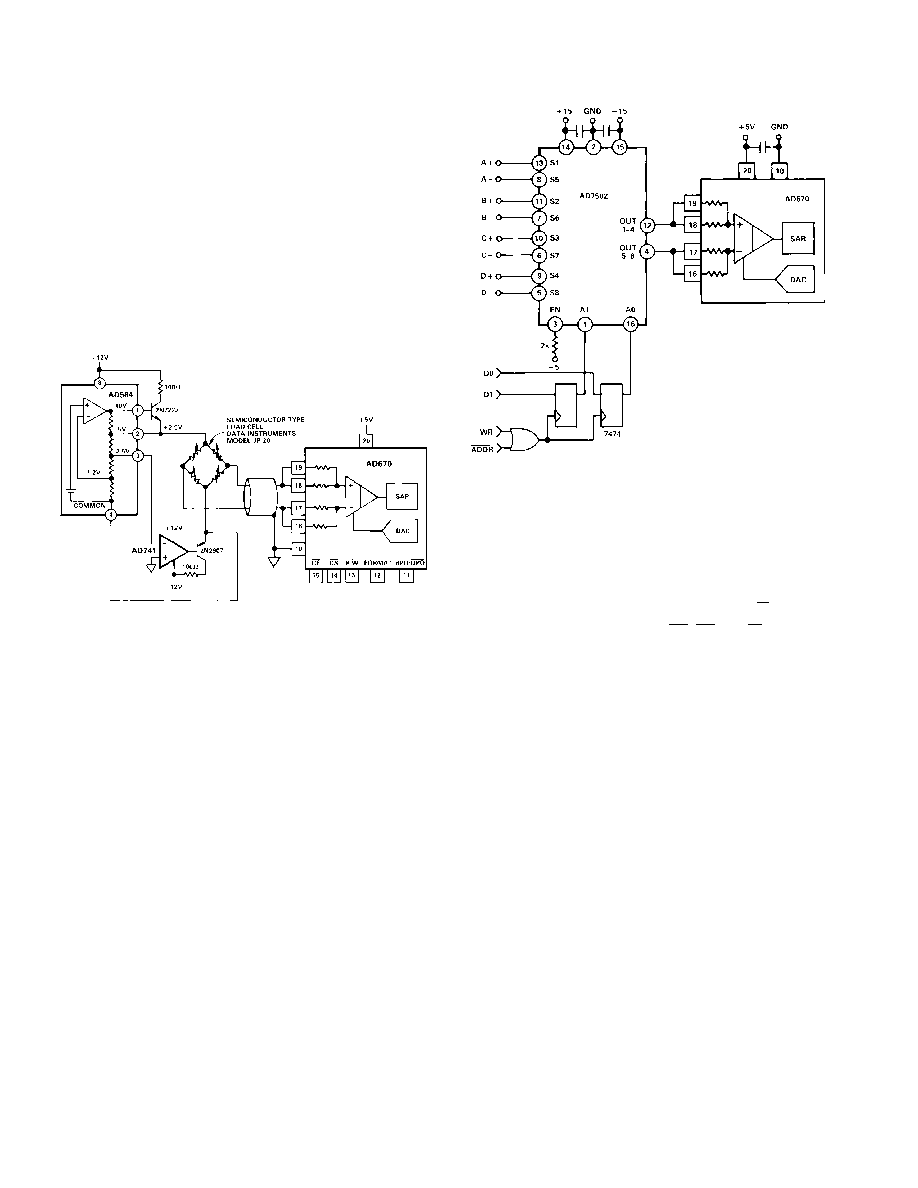
STRAIN GAGE MEASUREMENTS
Many semiconductor-type strain gages, pressure transducers,
and load cells may also be connected directly to the AD670.
These types of transducers typically produce 30 mV full-scale
per volt of excitation. In the circuit shown in Figure 15, the
AD670 is connected directly to a Data Instruments model JP-20
load cell. The AD584 programmable voltage reference is used
along with an AD741 op amp to provide the
±2.5 V excitation
for the load cell. The output of the transducer will be
±150 mV
for a force of
±20 pounds. The AD670 is configured for the
±128 millivolt range. The resolution is then approximately 2.1
ounces per LSB over a range of
±17 pounds. Scaling to exactly
2 ounces per LSB can be accomplished by trimming the refer-
ence voltage which excites the load cell.
Figure 15. AD670 Load Cell Interface
MULTIPLEXED INPUTS
Most data acquisition systems require the measurement of sev-
eral analog signals. Multiple A/D converters are often used to
digitize these inputs, requiring additional preamplification and
buffer stages per channel. Since these signals vary slowly, a dif-
ferential MUX can multiplex inputs from several transducers
into a single AD670. And since the AD670’s signal-conditioning
capability is preserved, the cost of several ADCs, differential
amplifiers, and other support components can be reduced to
that of a single AD670, a MUX, and a few digital logic gates.
An AD7502 dual 4-channel MUX appears in Figure 16 multi-
plexing four differential signals to the AD670. The AD7502’s
decoded address is gated with the microprocessor’s write signal
to provide a latching strobe at the flip-flops. A write cycle to the
AD7502’s address then latches the two LSBs of the data word
thereby selecting the input channel for subsequent conversions.
Figure 16. Multiplexed Analog Inputs to AD670
SAMPLED INPUTS
For those applications where the input signal is capable of slew-
ing more than 1/2 LSB during the AD670’s 10
s conversion
cycle, the input should be held constant for the cycle’s duration.
The circuit shown in Figure 17 uses a CMOS switch and two
capacitors to sample/hold the input. The AD670’s STATUS
output, once inverted, supplies the sample/hold (S/H) signal.
A convert command applied on the CE, CS or R/W lines will
initiate the conversion. The AD670’s STATUS output, once in-
verted, supplies the sample/hold signal to the CD4066. The
CD4066 CMOS switch shown in Figure 17 was chosen for its
fast transition times, low on-resistance and low cost. The con-
trol input’s propagation delay for switch-closed to switch-open
should remain less than 150 ns to ensure that the sample-to-
hold transition occurs before the first bit decision in the AD670.
相关PDF资料 |
PDF描述 |
|---|---|
| VE-J4W-MY-F3 | CONVERTER MOD DC/DC 5.5V 50W |
| VI-B4V-MX-F2 | CONVERTER MOD DC/DC 5.8V 75W |
| LTC2291CUP#PBF | IC ADC DUAL 12BIT 25MSPS 64QFN |
| VI-B4V-MX-F1 | CONVERTER MOD DC/DC 5.8V 75W |
| VE-J4V-MY-F2 | CONVERTER MOD DC/DC 5.8V 50W |
相关代理商/技术参数 |
参数描述 |
|---|---|
| AD670JNZ | 制造商:Analog Devices 功能描述:IC 8-BIT ADC |
| AD670JP | 功能描述:IC ADC 8BIT SGNL COND 20-PLCC RoHS:否 类别:集成电路 (IC) >> 数据采集 - 模数转换器 系列:- 产品培训模块:Lead (SnPb) Finish for COTS Obsolescence Mitigation Program 标准包装:2,500 系列:- 位数:12 采样率(每秒):3M 数据接口:- 转换器数目:- 功率耗散(最大):- 电压电源:- 工作温度:- 安装类型:表面贴装 封装/外壳:SOT-23-6 供应商设备封装:SOT-23-6 包装:带卷 (TR) 输入数目和类型:- |
| AD670JP-REEL | 制造商:Analog Devices 功能描述:ADC Single SAR 8-bit Parallel 20-Pin PLCC T/R |
| AD670JP-REEL7 | 制造商:Analog Devices 功能描述: |
| AD670JPZ | 功能描述:IC ADC 8BIT SIGNAL COND 20-PLCC RoHS:是 类别:集成电路 (IC) >> 数据采集 - 模数转换器 系列:- 标准包装:1 系列:- 位数:14 采样率(每秒):83k 数据接口:串行,并联 转换器数目:1 功率耗散(最大):95mW 电压电源:双 ± 工作温度:0°C ~ 70°C 安装类型:通孔 封装/外壳:28-DIP(0.600",15.24mm) 供应商设备封装:28-PDIP 包装:管件 输入数目和类型:1 个单端,双极 |
发布紧急采购,3分钟左右您将得到回复。