- 您现在的位置:买卖IC网 > PDF目录10278 > AD7262BSTZ-RL7 (Analog Devices Inc)IC ADC 12BIT W/PGA&COM 48-LQFP PDF资料下载
参数资料
| 型号: | AD7262BSTZ-RL7 |
| 厂商: | Analog Devices Inc |
| 文件页数: | 17/33页 |
| 文件大小: | 0K |
| 描述: | IC ADC 12BIT W/PGA&COM 48-LQFP |
| 标准包装: | 1 |
| 位数: | 12 |
| 采样率(每秒): | 1M |
| 数据接口: | DSP,MICROWIRE?,QSPI?,串行,SPI? |
| 转换器数目: | 2 |
| 功率耗散(最大): | 120mW |
| 电压电源: | 单电源 |
| 工作温度: | -40°C ~ 105°C |
| 安装类型: | 表面贴装 |
| 封装/外壳: | 48-LQFP |
| 供应商设备封装: | 48-LQFP(7x7) |
| 包装: | 标准包装 |
| 输入数目和类型: | 2 个差分,单极 |
| 产品目录页面: | 777 (CN2011-ZH PDF) |
| 其它名称: | AD7262BSTZ-RL7DKR |
第1页第2页第3页第4页第5页第6页第7页第8页第9页第10页第11页第12页第13页第14页第15页第16页当前第17页第18页第19页第20页第21页第22页第23页第24页第25页第26页第27页第28页第29页第30页第31页第32页第33页
AD7262
Rev. 0 | Page 23 of 32
Power-Up Conditions
On power-up, the status of the gain pins determine which mode
of operation is selected, as outlined in the Gain Selection section.
All registers are set to 0 by default.
If the AD7262/AD7262-5 are powered up in pin-driven mode,
the gain pins and the PDx pins should be configured to the
appropriate logic states and a calibration initiated if required.
Alternatively, if the AD7262/AD7262-5 are powered up in
control register mode, the comparators and ADCs are powered
down and the default gain is 1. Thus, powering up in control
register mode requires a write to the device to power up the
comparators and the ADCs.
It takes 15 μs to power up the AD7262/AD7262-5 when using
an external reference. When the internal reference is used, 240 μs
are required to power up the AD7262/AD7262-5 with a 1 μF
decoupling capacitor.
CONTROL REGISTER
The control register on the AD7262/AD7262-5 is a 12-bit read
and write register, which is used to control the device when not
in pin-driven mode. The PD0/DIN pin serves as the serial
DIN pin for the AD7262/AD7262-5 when the gain pins are set to
0 (that is, the part is not in pin-driven mode). The control
register can be used to select the gain of the PGAs, the power-
down modes, and the calibration of the offset for both ADC A
and ADC B. When operating in the control register mode, PD1
and PD2 should be connected to a low logic state.
These functions can also be implemented by setting the logic
levels on the gain pins, the power-down pins, and the CAL pin,
respectively. The control register can also be used to read the
offset and gain registers.
Data is loaded from the PD0/DIN pin of the AD7262/AD7262-5
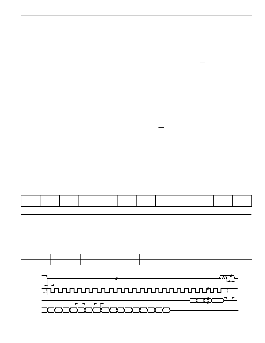
on the falling edge of SCLK when CS is in a logic low state. The
control register is selected by first writing the appropriate four
WR bits, as outlined in
. The 12 data bits must then be
clocked into the control register of the device. Thus, on the 16th
falling SCLK edge, the LSB is clocked into the device. One more
SCLK cycle is then required to write to the internal device
registers. In total, 17 SCLK cycles are required to successfully
write to the AD7262/AD7262-5. The data is transferred on the
PD0/DIN line while the conversion result is being processed.
The data transferred on the DIN line corresponds to the AD7262/
AD7262-5 configuration for the next conversion.
Only the information provided on the 12 falling clock edges
after the CS falling edge and the initial four write address bits is
loaded to the control register. The PD0/DIN pin should have a
logic low state for the four bits RD3 to RD0 when using the
control register to select the power-down modes or gain setting
or when initializing a calibration. The RD bits should also be set
to a logic low level to access the ADC results from both DOUTA
and DOUTB.
The power-up status of all bits is 0 and the MSB denotes the first
bit in the data stream. The bit functions are outlined in Table 8
and Table 9.
Table 8. Control Register Bits
MSB
LSB
Bit 11
Bit 10
Bit 9
Bit 8
Bit 7
Bit 6
Bit 5
Bit 4
Bit 3
Bit 2
Bit 1
Bit 0
RD3
RD2
RD1
RD0
CAL
PD2
PD1
PD0
G3
G2
G1
G0
Table 9. Control Register Bit Function Description
Bits
Mnemonic
Description
11 to 8
RD3 to RD0
Register address bits. These bits select which register the subsequent read is from. See Table 11.
7
CAL
Setting this bit high initiates an internal offset calibration. Once the calibration is completed, this pin can be reset low,
and the internal offset, which is stored in the on-chip offset registers, is automatically removed from the ADC results.
6 to 4
PD2 toPD0
Power-down bits. These bits select which power-down mode is programmed. See Table 7.
3 to 0
G3 to G0
Gain selection bits. These bits select which gain setting is used on the front-end PGA. See Table 6.
Table 10. Write Address Bits
WR3
WR2
WR1
WR0
Read Register Addressed
0
1
Control register
CS
SCLK
DOUTA
PD0/DIN
10
14
16
THREE-STATE
11
12
13
17
THREE-
STATE
15
DB10
DB11
18
20
19
30
31
DB0
THREE-STATE
WR1
WR0
RD3
RD2
RD1
RD0
CAL
PD2
PD1
PD0
G3
G2
G1
G0
WR2
WR3
t2
t8
tQUIET
9
8
7
6
5
4
3
2
1
t13
t14
07
60
6-
0
30
Figure 30. Timing Diagram for a Write Operation to the Control Register
相关PDF资料 |
PDF描述 |
|---|---|
| D38999/20KC98AA | CONN HSG RCPT 10POS WALL MT PINS |
| V24B3V3H150BL2 | CONVERTER MOD DC/DC 3.3V 150W |
| MS27472T18C32P | CONN RCPT 32POS WALL MT W/PINS |
| VE-JNH-MX-S | CONVERTER MOD DC/DC 52V 75W |
| MS27473E10F13SD | CONN PLUG 13POS STRAIGHT W/SCKT |
相关代理商/技术参数 |
参数描述 |
|---|---|
| AD7264 | 制造商:AD 制造商全称:Analog Devices 功能描述:1 MSPS, 14-Bit, Simultaneous Sampling SAR ADC with PGA and Four Comparators |
| AD7264BCPZ | 功能描述:IC ADC 14BIT 2CH 1MSPS 48LFCSP RoHS:是 类别:集成电路 (IC) >> 数据采集 - 模数转换器 系列:- 标准包装:1,000 系列:- 位数:12 采样率(每秒):300k 数据接口:并联 转换器数目:1 功率耗散(最大):75mW 电压电源:单电源 工作温度:0°C ~ 70°C 安装类型:表面贴装 封装/外壳:24-SOIC(0.295",7.50mm 宽) 供应商设备封装:24-SOIC 包装:带卷 (TR) 输入数目和类型:1 个单端,单极;1 个单端,双极 |
| AD7264BCPZ-5 | 功能描述:IC ADC 14BIT 2CH 500KSPS 48LFCSP RoHS:是 类别:集成电路 (IC) >> 数据采集 - 模数转换器 系列:- 标准包装:1,000 系列:- 位数:16 采样率(每秒):45k 数据接口:串行 转换器数目:2 功率耗散(最大):315mW 电压电源:模拟和数字 工作温度:0°C ~ 70°C 安装类型:表面贴装 封装/外壳:28-SOIC(0.295",7.50mm 宽) 供应商设备封装:28-SOIC W 包装:带卷 (TR) 输入数目和类型:2 个单端,单极 |
| AD7264BCPZ-5-RL7 | 功能描述:IC ADC 14BIT 2CH 500KSPS 48LFCSP RoHS:是 类别:集成电路 (IC) >> 数据采集 - 模数转换器 系列:- 标准包装:1,000 系列:- 位数:16 采样率(每秒):45k 数据接口:串行 转换器数目:2 功率耗散(最大):315mW 电压电源:模拟和数字 工作温度:0°C ~ 70°C 安装类型:表面贴装 封装/外壳:28-SOIC(0.295",7.50mm 宽) 供应商设备封装:28-SOIC W 包装:带卷 (TR) 输入数目和类型:2 个单端,单极 |
| AD7264BCPZ-RL7 | 功能描述:IC ADC 14BIT 2CH 1MSPS 48LFCSP RoHS:是 类别:集成电路 (IC) >> 数据采集 - 模数转换器 系列:- 标准包装:1,000 系列:- 位数:16 采样率(每秒):45k 数据接口:串行 转换器数目:2 功率耗散(最大):315mW 电压电源:模拟和数字 工作温度:0°C ~ 70°C 安装类型:表面贴装 封装/外壳:28-SOIC(0.295",7.50mm 宽) 供应商设备封装:28-SOIC W 包装:带卷 (TR) 输入数目和类型:2 个单端,单极 |
发布紧急采购,3分钟左右您将得到回复。