- 您现在的位置:买卖IC网 > PDF目录10689 > AD7266BCPZ-REEL7 (Analog Devices Inc)IC ADC 12BIT 2MSPS 3CH 32LFCSP PDF资料下载
参数资料
| 型号: | AD7266BCPZ-REEL7 |
| 厂商: | Analog Devices Inc |
| 文件页数: | 17/29页 |
| 文件大小: | 0K |
| 描述: | IC ADC 12BIT 2MSPS 3CH 32LFCSP |
| 设计资源: | AD7266 SAR ADC in DC-Coupled Differential and Single-Ended Appls (CN0039) |
| 标准包装: | 1 |
| 位数: | 12 |
| 采样率(每秒): | 2M |
| 数据接口: | DSP,MICROWIRE?,QSPI?,串行,SPI? |
| 转换器数目: | 2 |
| 功率耗散(最大): | 33.6mW |
| 电压电源: | 模拟和数字 |
| 工作温度: | -40°C ~ 125°C |
| 安装类型: | 表面贴装 |
| 封装/外壳: | 32-VFQFN 裸露焊盘,CSP |
| 供应商设备封装: | 32-LFCSP-VQ(5x5) |
| 包装: | 标准包装 |
| 输入数目和类型: | 12 个单端,单极;6 个差分,单极;6 个伪差分,单极 |
| 其它名称: | AD7266BCPZ-REEL7DKR |
第1页第2页第3页第4页第5页第6页第7页第8页第9页第10页第11页第12页第13页第14页第15页第16页当前第17页第18页第19页第20页第21页第22页第23页第24页第25页第26页第27页第28页第29页
AD7266
Rev. B | Page 23 of 28
MICROPROCESSOR INTERFACING
The serial interface on the AD7266 allows the part to be directly
connected to a range of many different microprocessors. This
section explains how to interface the AD7266 with some of the
more common microcontroller and DSP serial interface
protocols.
AD7266 TO ADSP-218x
The ADSP-218x family of DSPs interface directly to the
AD7266 without any glue logic required. The VDRIVE pin of the
AD7266 takes the same supply voltage as that of the ADSP-218x.
This allows the ADC to operate at a higher supply voltage than
its serial interface and therefore, the ADSP-218x, if necessary.
This example shows both DOUTA and DOUTB of the AD7266
connected to both serial ports of the ADSP-218x. The SPORT0
and SPORT1 control registers should be set up as shown in
Table 7. SPORT0 Control Register Setup
Setting
Description
TFSW = RFSW = 1
Alternate framing
INVRFS = INVTFS = 1
Active low frame signal
DTYPE = 00
Right justify data
SLEN = 1111
16-bit data-word (or may be set to
1101 for 14-bit data-word)
ISCLK = 1
Internal serial clock
TFSR = RFSR = 1
Frame every word
IRFS = 0
ITFS = 1
Table 8. SPORT1 Control Register Setup
Setting
Description
TFSW = RFSW = 1
Alternate framing
INVRFS = INVTFS = 1
Active low frame signal
DTYPE = 00
Right justify data
SLEN = 1111
16-bit data-word (or may be set to
1101 for 14-bit data-word)
ISCLK = 0
External serial clock
TFSR = RFSR = 1
Frame every word
IRFS = 0
ITFS = 1
To implement the power-down modes, SLEN should be set to
1001 to issue an 8-bit SCLK burst.
The connection diagram is shown in Figure 43. The ADSP-218x
has the TFS0 and RFS0 of the SPORT0 and the RFS1 of SPORT1
tied together. TFS0 is set as an output, and both RFS0 and RFS1
are set as inputs. The DSP operates in alternate framing mode,
and the SPORT control register is set up as described. The
frame synchronization signal generated on the TFS is tied to
CS, and as with all signal processing applications, equidistant
sampling is necessary. However, in this example, the timer
interrupt is used to control the sampling rate of the ADC and,
under certain conditions, equidistant sampling may not be
achieved.
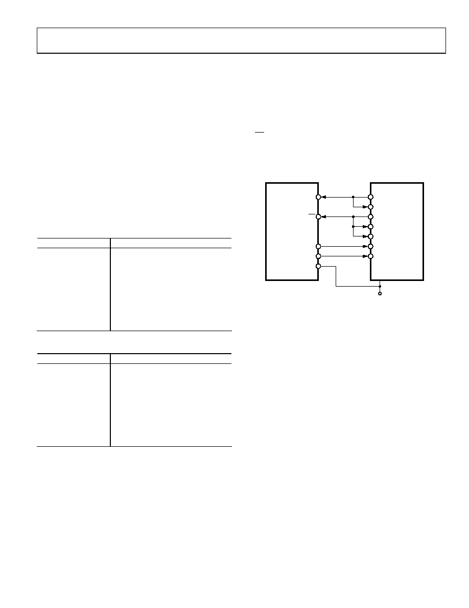
AD72661
SCLK
CS
ADSP-218x1
1ADDITIONAL PINS OMITTED FOR CLARITY.
SCLK0
DR0
RFS0
TFS0
DOUTA
VDRIVE
VDD
DOUTB
DR1
RFS1
SCLK1
04
60
3-
0
36
Figure 43. Interfacing the AD7266 to the ADSP-218x
The timer registers are loaded with a value that provides an
interrupt at the required sample interval. When an interrupt is
received, a value is transmitted with TFS/DT (ADC control
word). The TFS is used to control the RFS, and hence, the
reading of data. The frequency of the serial clock is set in the
SCLKDIV register. When the instruction to transmit with TFS
is given (AX0 = TX0), the state of the SCLK is checked. The
DSP waits until the SCLK has gone high, low, and high again
before transmission starts. If the timer and SCLK values are
chosen such that the instruction to transmit occurs on or near
the rising edge of SCLK, then the data may be transmitted or it
may wait until the next clock edge.
For example, the ADSP-2111 has a master clock frequency of
16 MHz. If the SCLKDIV register is loaded with the value 3,
then an SCLK of 2 MHz is obtained, and eight master clock
periods will elapse for every one SCLK period. If the timer
registers are loaded with the value 803, then 100.5 SCLKs will
occur between interrupts and, subsequently, between transmit
instructions. This situation yields sampling that is not equidistant
as the transmit instruction is occurring on an SCLK edge. If the
number of SCLKs between interrupts is a whole integer figure
of N, then equidistant sampling will be implemented by the DSP.
相关PDF资料 |
PDF描述 |
|---|---|
| ICL3222CAZ | TRANSMITTER/RCVR RS232 LP 20SSOP |
| ICL3222EIBZ | IC 2DRVR/2RCVR RS232 3V 18-SOIC |
| LTC1443CS#PBF | IC COMP W/REF LOWPWR QUAD 16SOIC |
| ICL3222CVZ | IC TXRX DL RS232 3-5.5V 20TSSOP |
| LTC2496CUHF#PBF | IC ADC 16BIT DELTA SIG 38-QFN |
相关代理商/技术参数 |
参数描述 |
|---|---|
| AD7266BSU | 制造商:Analog Devices 功能描述:ADC DUAL SAR 2MSPS 12-BIT SERL 32TQFP - Bulk |
| AD7266BSUZ | 功能描述:IC ADC 12BIT 3CH 2MSPS 32-TQFP RoHS:是 类别:集成电路 (IC) >> 数据采集 - 模数转换器 系列:- 标准包装:1,000 系列:- 位数:12 采样率(每秒):300k 数据接口:并联 转换器数目:1 功率耗散(最大):75mW 电压电源:单电源 工作温度:0°C ~ 70°C 安装类型:表面贴装 封装/外壳:24-SOIC(0.295",7.50mm 宽) 供应商设备封装:24-SOIC 包装:带卷 (TR) 输入数目和类型:1 个单端,单极;1 个单端,双极 |
| AD7266BSUZ-REEL | 功能描述:IC ADC 12BIT 3CHAN 2MSPS 32TQFP RoHS:是 类别:集成电路 (IC) >> 数据采集 - 模数转换器 系列:- 标准包装:1,000 系列:- 位数:16 采样率(每秒):45k 数据接口:串行 转换器数目:2 功率耗散(最大):315mW 电压电源:模拟和数字 工作温度:0°C ~ 70°C 安装类型:表面贴装 封装/外壳:28-SOIC(0.295",7.50mm 宽) 供应商设备封装:28-SOIC W 包装:带卷 (TR) 输入数目和类型:2 个单端,单极 |
| AD7266BSUZ-REEL7 | 功能描述:IC ADC 12BIT 3CHAN 2MSPS 32TQFP RoHS:是 类别:集成电路 (IC) >> 数据采集 - 模数转换器 系列:- 标准包装:1,000 系列:- 位数:16 采样率(每秒):45k 数据接口:串行 转换器数目:2 功率耗散(最大):315mW 电压电源:模拟和数字 工作温度:0°C ~ 70°C 安装类型:表面贴装 封装/外壳:28-SOIC(0.295",7.50mm 宽) 供应商设备封装:28-SOIC W 包装:带卷 (TR) 输入数目和类型:2 个单端,单极 |
| AD7273 | 制造商:AD 制造商全称:Analog Devices 功能描述:3MSPS,10-/12-Bit ADCs in 8-Lead TSOT |
发布紧急采购,3分钟左右您将得到回复。