- 您现在的位置:买卖IC网 > PDF目录10689 > AD7266BCPZ-REEL7 (Analog Devices Inc)IC ADC 12BIT 2MSPS 3CH 32LFCSP PDF资料下载
参数资料
| 型号: | AD7266BCPZ-REEL7 |
| 厂商: | Analog Devices Inc |
| 文件页数: | 18/29页 |
| 文件大小: | 0K |
| 描述: | IC ADC 12BIT 2MSPS 3CH 32LFCSP |
| 设计资源: | AD7266 SAR ADC in DC-Coupled Differential and Single-Ended Appls (CN0039) |
| 标准包装: | 1 |
| 位数: | 12 |
| 采样率(每秒): | 2M |
| 数据接口: | DSP,MICROWIRE?,QSPI?,串行,SPI? |
| 转换器数目: | 2 |
| 功率耗散(最大): | 33.6mW |
| 电压电源: | 模拟和数字 |
| 工作温度: | -40°C ~ 125°C |
| 安装类型: | 表面贴装 |
| 封装/外壳: | 32-VFQFN 裸露焊盘,CSP |
| 供应商设备封装: | 32-LFCSP-VQ(5x5) |
| 包装: | 标准包装 |
| 输入数目和类型: | 12 个单端,单极;6 个差分,单极;6 个伪差分,单极 |
| 其它名称: | AD7266BCPZ-REEL7DKR |
第1页第2页第3页第4页第5页第6页第7页第8页第9页第10页第11页第12页第13页第14页第15页第16页第17页当前第18页第19页第20页第21页第22页第23页第24页第25页第26页第27页第28页第29页
AD7266
Rev. B | Page 24 of 28
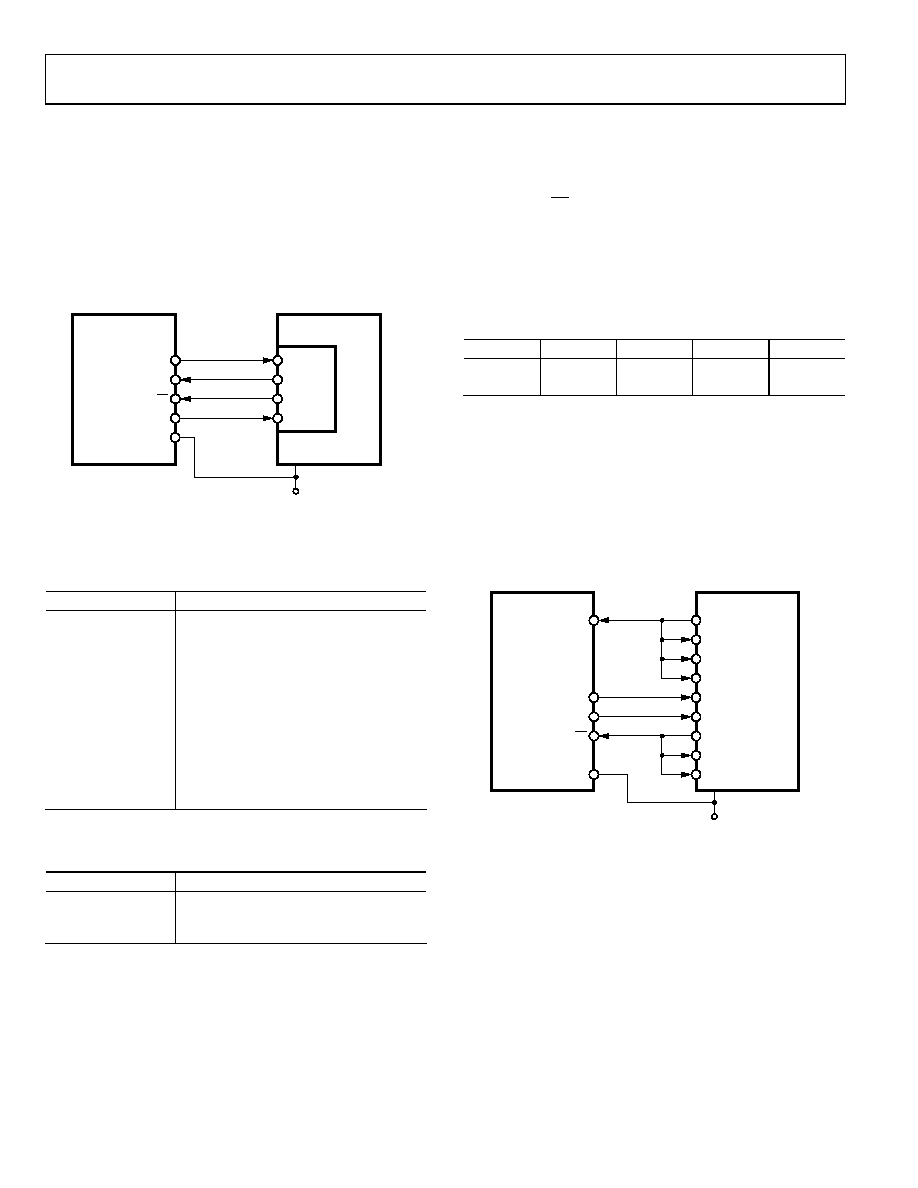
AD7266 TO ADSP-BF53x
The ADSP-BF53x family of DSPs interface directly to the
AD7266 without any glue logic required. The availability of
secondary receive registers on the serial ports of the Blackfin
DSPs means only one serial port is necessary to read from both
DOUTB of the AD7266 connected to Serial Port 0 of the
ADSP-BF53x. The SPORT0 Receive Configuration 1 register
and SPORT0 Receive Configuration 2 register should be set up
as outlined in Table 9 and Table 10.
SERIAL
DEVICE A
(PRIMARY)
SERIAL
DEVICE B
(SECONDARY)
AD72661
DOUTA
CS
SCLK
ADSP-BF53x1
1ADDITIONAL PINS OMITTED FOR CLARITY.
DR0PRI
DR0SEC
RFS0
VDRIVE
VDD
DOUTB
RCLK0
04603-037
SPORT0
Figure 44. Interfacing the AD7266 to the ADSP-BF53x
Table 9. The SPORT0 Receive Configuration 1 Register
(SPORT0_RCR1)
Setting
Description
RCKFE = 1
Sample data with falling edge of RSCLK
LRFS = 1
Active low frame signal
RFSR = 1
Frame every word
IRFS = 1
Internal RFS used
RLSBIT = 0
Receive MSB first
RDTYPE = 00
Zero fill
IRCLK = 1
Internal receive clock
RSPEN = 1
Receive enabled
SLEN = 1111
16-bit data-word (or may be set to 1101
for 14-bit data-word)
TFSR = RFSR = 1
Table 10. The SPORT0 Receive Configuration 2 Register
(SPORT0_RCR2)
Setting
Description
RXSE = 1
Secondary side enabled
SLEN = 1111
16-bit data-word ( or may be set to 1101
for 14-bit data-word)
To implement the power-down modes, SLEN should be set to
1001 to issue an 8-bit SCLK burst. A Blackfin driver for the
AD7266 is available to download at www.analog.com.
AD7266 TO TMS320C541
The serial interface on the TMS320C541 uses a continuous
serial clock and frame synchronization signals to synchronize
the data transfer operations with peripheral devices like the
AD7266. The CS input allows easy interfacing between the
TMS320C541 and the AD7266 without any glue logic required.
The serial ports of the TMS320C541 are set up to operate in
burst mode with internal CLKX0 (TX serial clock on Serial
Port 0) and FSX0 (TX frame sync from Serial Port 0). The serial
port control registers (SPC) must have the following setup.
Table 11. Serial Port Control Register Set Up
SPC
FO
FSM
MCM
TXM
SPC0
0
1
SPC1
0
1
0
The format bit, FO, may be set to 1 to set the word length to
8 bits to implement the power-down modes on the AD7266.
The connection diagram is shown in Figure 45. It is imperative
that for signal processing applications, the frame synchroniza-
tion signal from the TMS320C541 provides equidistant sampling.
The VDRIVE pin of the AD7266 takes the same supply voltage as
that of the TMS320C541. This allows the ADC to operate at a
higher voltage than its serial interface and therefore, the
TMS320C541, if necessary.
FSR1
FSR0
AD72661
SCLK
TMS320C5411
1ADDITIONAL PINS OMITTED FOR CLARITY.
CLKX0
DR1
CLKR1
CLKX1
DOUTB
DOUTA
VDRIVE
VDD
CS
FSX0
DR0
CLKR0
04603-038
Figure 45. Interfacing the AD7266 to the TMS320C541
相关PDF资料 |
PDF描述 |
|---|---|
| ICL3222CAZ | TRANSMITTER/RCVR RS232 LP 20SSOP |
| ICL3222EIBZ | IC 2DRVR/2RCVR RS232 3V 18-SOIC |
| LTC1443CS#PBF | IC COMP W/REF LOWPWR QUAD 16SOIC |
| ICL3222CVZ | IC TXRX DL RS232 3-5.5V 20TSSOP |
| LTC2496CUHF#PBF | IC ADC 16BIT DELTA SIG 38-QFN |
相关代理商/技术参数 |
参数描述 |
|---|---|
| AD7266BSU | 制造商:Analog Devices 功能描述:ADC DUAL SAR 2MSPS 12-BIT SERL 32TQFP - Bulk |
| AD7266BSUZ | 功能描述:IC ADC 12BIT 3CH 2MSPS 32-TQFP RoHS:是 类别:集成电路 (IC) >> 数据采集 - 模数转换器 系列:- 标准包装:1,000 系列:- 位数:12 采样率(每秒):300k 数据接口:并联 转换器数目:1 功率耗散(最大):75mW 电压电源:单电源 工作温度:0°C ~ 70°C 安装类型:表面贴装 封装/外壳:24-SOIC(0.295",7.50mm 宽) 供应商设备封装:24-SOIC 包装:带卷 (TR) 输入数目和类型:1 个单端,单极;1 个单端,双极 |
| AD7266BSUZ-REEL | 功能描述:IC ADC 12BIT 3CHAN 2MSPS 32TQFP RoHS:是 类别:集成电路 (IC) >> 数据采集 - 模数转换器 系列:- 标准包装:1,000 系列:- 位数:16 采样率(每秒):45k 数据接口:串行 转换器数目:2 功率耗散(最大):315mW 电压电源:模拟和数字 工作温度:0°C ~ 70°C 安装类型:表面贴装 封装/外壳:28-SOIC(0.295",7.50mm 宽) 供应商设备封装:28-SOIC W 包装:带卷 (TR) 输入数目和类型:2 个单端,单极 |
| AD7266BSUZ-REEL7 | 功能描述:IC ADC 12BIT 3CHAN 2MSPS 32TQFP RoHS:是 类别:集成电路 (IC) >> 数据采集 - 模数转换器 系列:- 标准包装:1,000 系列:- 位数:16 采样率(每秒):45k 数据接口:串行 转换器数目:2 功率耗散(最大):315mW 电压电源:模拟和数字 工作温度:0°C ~ 70°C 安装类型:表面贴装 封装/外壳:28-SOIC(0.295",7.50mm 宽) 供应商设备封装:28-SOIC W 包装:带卷 (TR) 输入数目和类型:2 个单端,单极 |
| AD7273 | 制造商:AD 制造商全称:Analog Devices 功能描述:3MSPS,10-/12-Bit ADCs in 8-Lead TSOT |
发布紧急采购,3分钟左右您将得到回复。