参数资料
| 型号: | AD7291BCPZ-RL7 |
| 厂商: | Analog Devices Inc |
| 文件页数: | 15/29页 |
| 文件大小: | 0K |
| 描述: | IC ADC I2C/SRL 22.22K 20LFCSP |
| 标准包装: | 1,500 |
| 位数: | 12 |
| 采样率(每秒): | 22.22k |
| 数据接口: | I²C,串行 |
| 转换器数目: | 1 |
| 功率耗散(最大): | 12.6mW |
| 电压电源: | 单电源 |
| 工作温度: | -40°C ~ 125°C |
| 安装类型: | 表面贴装 |
| 封装/外壳: | 20-WFQFN 裸露焊盘,CSP |
| 供应商设备封装: | 20-LFCSP-WQ(4x4) |
| 包装: | 带卷 (TR) |
| 输入数目和类型: | 8 个单端,单极 |
| 配用: | EVAL-AD7291SDZ-ND - BOARD EVAL FOR AD7291 |
第1页第2页第3页第4页第5页第6页第7页第8页第9页第10页第11页第12页第13页第14页当前第15页第16页第17页第18页第19页第20页第21页第22页第23页第24页第25页第26页第27页第28页第29页
Data Sheet
AD7291
Rev. B | Page 21 of 28
I2C INTERFACE
Control of the AD7291 is carried out via the I2C compatible
serial bus. The AD7291 is connected to this bus as a slave device
under the control of a master device such as the processor.
SERIAL BUS ADDRESS BYTE
The first byte the user writes to the device is the slave address
byte. Similar to all I2C-compatible devices, the AD7291 has a
7-bit serial address. The three MSBs of this address are set to
010. The four LSBs are user-programmable by the three-state
input pins, AS0 and AS1, as shown in Table 31.
to GND, and NC refers to a pin left floating. Note that in this
final case, the stray capacitance on the pin must be less than
30 pF to allow correct detection of the floating state; therefore,
any PCB trace must be kept as short as possible.
Table 31. Slave Address Control Using Three-State Input Pins
Slave Address (A6 to A0)
AS1
AS0
Binary
Hex
H
010 0000
0x20
H
NC
010 0010
0x22
H
L
010 0011
0x23
NC
H
010 1000
0x28
NC
010 1010
0x2A
NC
L
010 1011
0x2B
L
H
010 1100
0x2C
L
NC
010 1110
0x2E
L
010 1111
0x2F
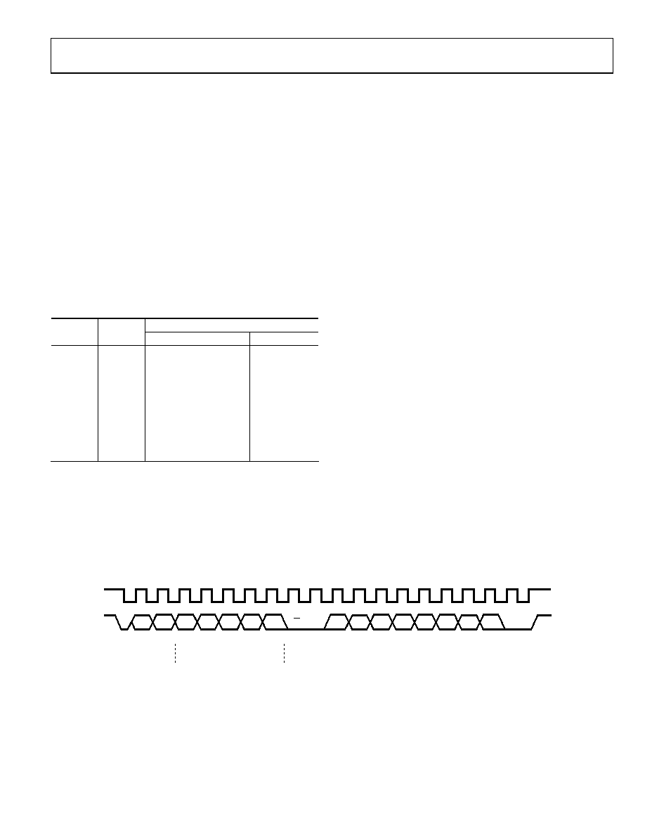
GENERAL I2C TIMING
Figure 24 shows the timing diagram for general read and write
operations using an I2C-compliant interface.
When no device is driving the bus, both SCL and SDA are high.
This is known as the idle state. When the bus is idle, the master
initiates a data transfer by establishing a start condition, defined
as a high-to-low transition on the serial data line (SDA) while
the serial clock line (SCL) remains high. This indicates that a
data stream follows. The master device is responsible for
generating the clock.
Data is sent over the serial bus in groups of nine bits—eight bits
of data from the transmitter followed by an acknowledge bit
(ACK) from the receiver. Data transitions on the SDA line must
occur during the low period of the clock signal and remain
stable during the high period. The receiver should pull the SDA
line low during the acknowledge bit to signal that the preceding
byte has been received correctly. If this is not the case, cancel
the transaction.
The first byte that the master sends must consist of a 7-bit slave
address, followed by a data direction bit. Each device on the
bus has a unique slave address; therefore, the first byte sets up
communication with a single slave device for the duration of the
transaction.
The transaction can be used either to write to a slave device
(data direction bit = 0) or to read data from it (data direction
bit = 1). In the case of a read transaction, it is often necessary
first to write to the slave device (in a separate write transaction)
to tell it from which register to read. Reading and writing
cannot be combined in one transaction.
When the transaction is complete, the master can keep control
of the bus, initiating a new transaction by generating another
start bit (high-to-low transition on SDA while SCL is high).
This is known as a repeated start (SR). Alternatively, the bus
can be relinquished by releasing the SCL line followed by the
SDA line. This low-to-high transition on SDA while SCL is high
is known as a stop bit (P), and it leaves the I2C bus in its idle
state (no current is consumed by the bus).
The example in Figure 24 shows a simple write transaction
with an AD7291 as the slave device. In this example, the
AD7291 register pointer is being set up for a future read
transaction.
P7
P6
P5
P4
P3
P2
P1
P0
START COND
BY MASTER
ACK. BY
AD7291
SLAVE ADDRESS BYTE
ACK. BY
AD7291
SCL
SDA
REGISTER ADDRESS
STOP BY
MASTER
USER PROGRAMMABLE 5 LSBs
R/W
A6
A5
A4
A3
A2
A1
A0
0
87
11
-0
40
Figure 24. General I2C Timing
相关PDF资料 |
PDF描述 |
|---|---|
| AD7298-1BCPZ-RL | IC ADC 10BIT SPI/SRL 8CH 20LFCSP |
| AD7298BCPZ-RL7 | IC ADC 10BIT SPI/SRL 8CH 20LFCSP |
| AD7302BRUZ-REEL7 | IC DAC 8BIT DUAL R-R 20-TSSOP |
| AD7303BRM | IC DAC 8BIT DUAL R-R 8-MSOP |
| AD7305BRU | IC DAC 8BIT QUAD R-R 20-TSSOP |
相关代理商/技术参数 |
参数描述 |
|---|---|
| AD7291TCPZ-EP | 功能描述:CH 12 BIT SAR WT INTERNAL TEMP S 制造商:analog devices inc. 系列:- 包装:托盘 零件状态:在售 位数:12 采样率(每秒):22.22k 输入数:8 输入类型:单端 数据接口:I2C 配置:MUX-S/H-ADC 无线电 - S/H:ADC:1:1 A/D 转换器数:1 架构:SAR 参考类型:外部, 内部 电压 - 电源,模拟:2.8 V ~ 3.6 V 电压 - 电源,数字:2.8 V ~ 3.6 V 特性:温度传感器 工作温度:-55°C ~ 125°C(TA) 封装/外壳:20-WFQFN 裸露焊盘,CSP 供应商器件封装:20-LFCSP(4x4) 标准包装:1 |
| AD7291TCPZ-EP-RL7 | 功能描述:8 CH 12 BIT SAR WT INTERNAL TEMP 制造商:analog devices inc. 系列:- 包装:带卷(TR) 零件状态:在售 位数:12 采样率(每秒):22.22k 输入数:8 输入类型:单端 数据接口:I2C 配置:MUX-S/H-ADC 无线电 - S/H:ADC:1:1 A/D 转换器数:1 架构:SAR 参考类型:外部, 内部 电压 - 电源,模拟:2.8 V ~ 3.6 V 电压 - 电源,数字:2.8 V ~ 3.6 V 特性:温度传感器 工作温度:-55°C ~ 125°C(TA) 封装/外壳:20-WFQFN 裸露焊盘,CSP 供应商器件封装:20-LFCSP(4x4) 标准包装:1,500 |
| AD7292BCPZ | 制造商:Analog Devices 功能描述:Monitor and Control System 36-Pin LFCSP EP Tray 制造商:Analog Devices 功能描述:12-BIT,MULTI-CHANNEL, ADC,DAC WT TEMP IC - Trays 制造商:Analog Devices 功能描述:IC ADC 10BIT SPI/SRL 36-LFCSP 制造商:Analog Devices 功能描述:ADC DAC TEMP SENSOR GPIO 3 制造商:Analog Devices 功能描述:ADC, DAC, TEMP SENSOR, GPIO, 36LFCSP 制造商:Analog Devices Inc. 功能描述:Analog to Digital Converters - ADC 12-Bit Multi-Channel ADC DAC wt Temp IC 制造商:Analog Devices 功能描述:ANALOGUE MONITORING & CONTROL CIRCUIT, LFCSP-36; IC Function:Analogue Monitoring and Control Circuit; Supply Voltage Min:1.8V; Supply Voltage Max:5.25V; Operating Temperature Min:-40C; Operating Temperature Max:125C; No. of Pins:36;RoHS Compliant: Yes |
| AD7292BCPZ-RL | 制造商:Analog Devices 功能描述:Monitor and Control System 36-Pin LFCSP EP T/R 制造商:Analog Devices 功能描述:12-BIT,MULTI-CHANNEL, ADC,DAC WT TEMP IC - Tape and Reel 制造商:Analog Devices 功能描述:IC ADC 10BIT SPI/SRL 36LFCSP 制造商:Analog Devices Inc. 功能描述:Analog to Digital Converters - ADC 12-Bit Multi-Channel ADC DAC wt Temp IC 制造商:Analog Devices Inc. 功能描述:Analog to Digital Converters - ADC 10B Monitor & Cntrl System w/ Temp Sensr |
| AD7293BCPZ | 功能描述:12-BIT POWER AMPLIFIER CURRENT C 制造商:analog devices inc. 系列:* 零件状态:有效 标准包装:1 |
发布紧急采购,3分钟左右您将得到回复。