参数资料
| 型号: | AD7291BCPZ-RL7 |
| 厂商: | Analog Devices Inc |
| 文件页数: | 28/29页 |
| 文件大小: | 0K |
| 描述: | IC ADC I2C/SRL 22.22K 20LFCSP |
| 标准包装: | 1,500 |
| 位数: | 12 |
| 采样率(每秒): | 22.22k |
| 数据接口: | I²C,串行 |
| 转换器数目: | 1 |
| 功率耗散(最大): | 12.6mW |
| 电压电源: | 单电源 |
| 工作温度: | -40°C ~ 125°C |
| 安装类型: | 表面贴装 |
| 封装/外壳: | 20-WFQFN 裸露焊盘,CSP |
| 供应商设备封装: | 20-LFCSP-WQ(4x4) |
| 包装: | 带卷 (TR) |
| 输入数目和类型: | 8 个单端,单极 |
| 配用: | EVAL-AD7291SDZ-ND - BOARD EVAL FOR AD7291 |
第1页第2页第3页第4页第5页第6页第7页第8页第9页第10页第11页第12页第13页第14页第15页第16页第17页第18页第19页第20页第21页第22页第23页第24页第25页第26页第27页当前第28页第29页
Data Sheet
AD7291
Rev. B | Page 7 of 28
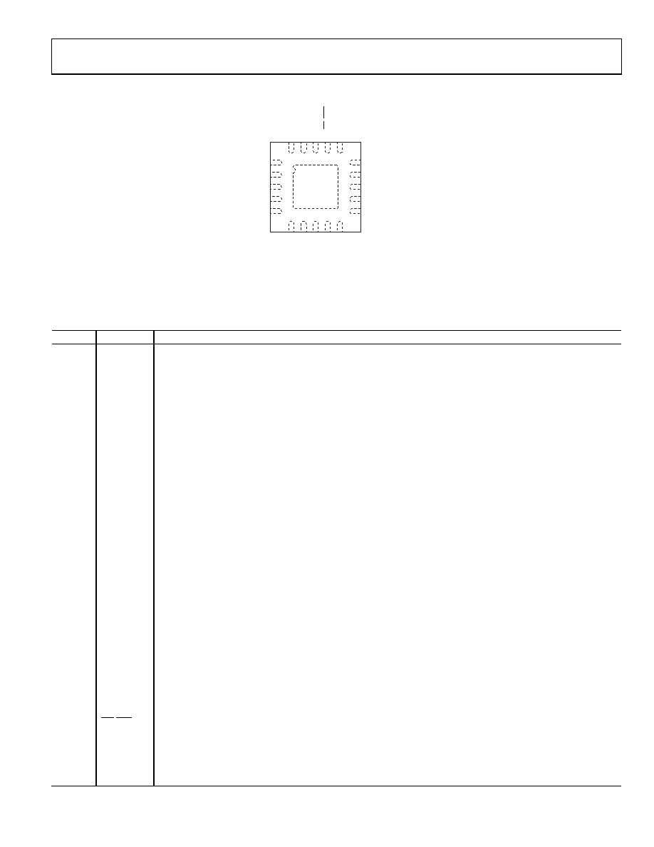
PIN CONFIGURATION AND FUNCTION DESCRIPTIONS
14
13
12
1
3
4
SDA
15
SCL
AS1
ALERT
11
AS0
VIN3
VIN5
2
VIN4
VIN6
5
VIN7
7
V
R
E
F
6
G
N
D
1
8
D
C
A
P
9
G
N
D
1
0
V
D
1
9
V
IN
1
2
0
V
IN
2
1
8
V
IN
0
1
7
P
D
/R
S
T
1
6
V
D
R
IV
E
AD7291
TOP VIEW
(Not to Scale)
08
7
1
1-
0
03
NOTES
1. THE EXPOSED METAL PADDLE ON THE BOTTOM
OF THE LFCSP PACKAGE SHOULD BE SOLDERED
TO PCB GROUND FOR PROPER HEAT DISSIPATION
AND PERFORMANCE.
Figure 3. Pin Configuration
Table 6. Pin Function Descriptions
Pin No.
Mnemonic
Description
1 to 5,
18 to 20
VIN3, VIN4,
VIN5, VIN6,
VIN7, VIN0,
VIN1, VIN2
Analog Inputs. The AD7291 has eight single-ended analog inputs that are multiplexed into the on-chip track-and-
hold amplifier. Each input channel can accept analog inputs from 0 V to 2.5 V. Any unused input channels should
be connected to GND1 to avoid noise pickup.
6
GND1
Ground. Ground reference point for the internal reference circuitry on the AD7291. All analog input signals and
the external reference signals should be referred to this GND1 voltage. The GND1 pin should be connected to the
ground plane of a system. All ground pins should ideally be at the same potential and must not be more than 0.3 V
apart, even on a transient basis. The VREF pin should be decoupled to this ground pin via a 10 μF decoupling
capacitor.
7
VREF
Internal Reference/External Reference Supply. The nominal internal reference voltage of 2.5 V appears at this pin.
Provided the output is buffered, the on-chip reference can be taken from this pin and applied externally to the rest
of a system. Decoupling capacitors should be connected to this pin to decouple the reference buffer. For best
performance, it is recommended to use a 10 μF decoupling capacitor on this pin to GND1. The internal reference
can be disabled and an external reference supplied to this pin if required. The input voltage range for the external
reference is 2.0 V to 2.5 V.
8
DCAP
Decoupling Capacitor Pin. Decoupling capacitors (1 μF recommended) are connected to this pin to decouple the
internal LDO.
9
GND
Ground. Ground reference point for all analog and digital circuitry on the AD7291. The GND pin should be con-
nected to the ground plane of the system. All ground pins should ideally be at the same potential and must not be
more than 0.3 V apart, even on a transient basis. Both DCAP and VDD pins should be decoupled to this GND pin.
10
VDD
Supply Voltage, 2.8 V to 3.6 V. This supply should be decoupled to GND with 10 μF and 100 nF decoupling capacitors.
11, 13
AS0, AS1
Logic Input. Together, the logic state of these two inputs selects a unique I2C address for the AD7291. See Table 31
for details. The device address depends on the voltage applied to these pins.
12
ALERT
Digital Output. This pin acts as an out-of-range indicator and, if enabled, becomes active when the conversion
result violates the DATAHIGH or DATALOW register values. See the Limit Registers (0x04 to 0x1E) section.
14
SDA
Digital Input/Output. Serial bus bidirectional data. This open-drain output requires a pull-up resistor. The output coding
is straight binary for the voltage channels and twos complement for the temperature sensor result.
15
SCL
Digital Input. Serial I2C Bus Clock. This input requires a pull-up resistor. The data transfer rate in I2C mode is
compatible with both 100 kHz and 400 kHz operating modes.
16
VDRIVE
Logic Power Supply Input. The voltage supplied at this pin determines the voltage at which the interface operates.
This pin should be decoupled to GND. The voltage range on this pin is 1.65 V to 3.6 V and may be less than the
voltage at VDD but should never exceed it by more than 0.3 V.
17
PD/RST
Power-Down Pin. This pin places the part into a full power-down mode and enables power conservation when
operation is not required. This pin can be used to reset the device by toggling the pin low for a minimum of 1 ns and a
maximum of 100 ns. If the maximum time is exceeded, the part enters power-down mode. When placing the device in
full power-down mode, the analog inputs must be returned to 0 V.
EPAD
Exposed Paddle. The exposed metal paddle on the bottom of the LFCSP package should be soldered to PCB
ground for proper functionality and heat dissipation.
相关PDF资料 |
PDF描述 |
|---|---|
| AD7298-1BCPZ-RL | IC ADC 10BIT SPI/SRL 8CH 20LFCSP |
| AD7298BCPZ-RL7 | IC ADC 10BIT SPI/SRL 8CH 20LFCSP |
| AD7302BRUZ-REEL7 | IC DAC 8BIT DUAL R-R 20-TSSOP |
| AD7303BRM | IC DAC 8BIT DUAL R-R 8-MSOP |
| AD7305BRU | IC DAC 8BIT QUAD R-R 20-TSSOP |
相关代理商/技术参数 |
参数描述 |
|---|---|
| AD7291TCPZ-EP | 功能描述:CH 12 BIT SAR WT INTERNAL TEMP S 制造商:analog devices inc. 系列:- 包装:托盘 零件状态:在售 位数:12 采样率(每秒):22.22k 输入数:8 输入类型:单端 数据接口:I2C 配置:MUX-S/H-ADC 无线电 - S/H:ADC:1:1 A/D 转换器数:1 架构:SAR 参考类型:外部, 内部 电压 - 电源,模拟:2.8 V ~ 3.6 V 电压 - 电源,数字:2.8 V ~ 3.6 V 特性:温度传感器 工作温度:-55°C ~ 125°C(TA) 封装/外壳:20-WFQFN 裸露焊盘,CSP 供应商器件封装:20-LFCSP(4x4) 标准包装:1 |
| AD7291TCPZ-EP-RL7 | 功能描述:8 CH 12 BIT SAR WT INTERNAL TEMP 制造商:analog devices inc. 系列:- 包装:带卷(TR) 零件状态:在售 位数:12 采样率(每秒):22.22k 输入数:8 输入类型:单端 数据接口:I2C 配置:MUX-S/H-ADC 无线电 - S/H:ADC:1:1 A/D 转换器数:1 架构:SAR 参考类型:外部, 内部 电压 - 电源,模拟:2.8 V ~ 3.6 V 电压 - 电源,数字:2.8 V ~ 3.6 V 特性:温度传感器 工作温度:-55°C ~ 125°C(TA) 封装/外壳:20-WFQFN 裸露焊盘,CSP 供应商器件封装:20-LFCSP(4x4) 标准包装:1,500 |
| AD7292BCPZ | 制造商:Analog Devices 功能描述:Monitor and Control System 36-Pin LFCSP EP Tray 制造商:Analog Devices 功能描述:12-BIT,MULTI-CHANNEL, ADC,DAC WT TEMP IC - Trays 制造商:Analog Devices 功能描述:IC ADC 10BIT SPI/SRL 36-LFCSP 制造商:Analog Devices 功能描述:ADC DAC TEMP SENSOR GPIO 3 制造商:Analog Devices 功能描述:ADC, DAC, TEMP SENSOR, GPIO, 36LFCSP 制造商:Analog Devices Inc. 功能描述:Analog to Digital Converters - ADC 12-Bit Multi-Channel ADC DAC wt Temp IC 制造商:Analog Devices 功能描述:ANALOGUE MONITORING & CONTROL CIRCUIT, LFCSP-36; IC Function:Analogue Monitoring and Control Circuit; Supply Voltage Min:1.8V; Supply Voltage Max:5.25V; Operating Temperature Min:-40C; Operating Temperature Max:125C; No. of Pins:36;RoHS Compliant: Yes |
| AD7292BCPZ-RL | 制造商:Analog Devices 功能描述:Monitor and Control System 36-Pin LFCSP EP T/R 制造商:Analog Devices 功能描述:12-BIT,MULTI-CHANNEL, ADC,DAC WT TEMP IC - Tape and Reel 制造商:Analog Devices 功能描述:IC ADC 10BIT SPI/SRL 36LFCSP 制造商:Analog Devices Inc. 功能描述:Analog to Digital Converters - ADC 12-Bit Multi-Channel ADC DAC wt Temp IC 制造商:Analog Devices Inc. 功能描述:Analog to Digital Converters - ADC 10B Monitor & Cntrl System w/ Temp Sensr |
| AD7293BCPZ | 功能描述:12-BIT POWER AMPLIFIER CURRENT C 制造商:analog devices inc. 系列:* 零件状态:有效 标准包装:1 |
发布紧急采购,3分钟左右您将得到回复。