- 您现在的位置:买卖IC网 > PDF目录10672 > AD7328BRUZ (Analog Devices Inc)IC ADC 12BIT+ SAR 8CHAN 20TSSOP PDF资料下载
参数资料
| 型号: | AD7328BRUZ |
| 厂商: | Analog Devices Inc |
| 文件页数: | 26/37页 |
| 文件大小: | 0K |
| 描述: | IC ADC 12BIT+ SAR 8CHAN 20TSSOP |
| 设计资源: | Using AD7328 in Appls with Single-Ended Industrial-Level Signals (CN0047) |
| 标准包装: | 75 |
| 系列: | iCMOS® |
| 位数: | 12 |
| 采样率(每秒): | 1M |
| 数据接口: | DSP,MICROWIRE?,QSPI?,串行,SPI? |
| 转换器数目: | 1 |
| 功率耗散(最大): | 30mW |
| 电压电源: | 双 ± |
| 工作温度: | -40°C ~ 85°C |
| 安装类型: | 表面贴装 |
| 封装/外壳: | 20-TSSOP(0.173",4.40mm 宽) |
| 供应商设备封装: | 20-TSSOP |
| 包装: | 管件 |
| 输入数目和类型: | 8 个单端,单极;8 个单端,双极;4 个差分,单极;4 个差分,双极 |
| 产品目录页面: | 777 (CN2011-ZH PDF) |
第1页第2页第3页第4页第5页第6页第7页第8页第9页第10页第11页第12页第13页第14页第15页第16页第17页第18页第19页第20页第21页第22页第23页第24页第25页当前第26页第27页第28页第29页第30页第31页第32页第33页第34页第35页第36页第37页
Data Sheet
AD7328
Rev. C | Page 31 of 36
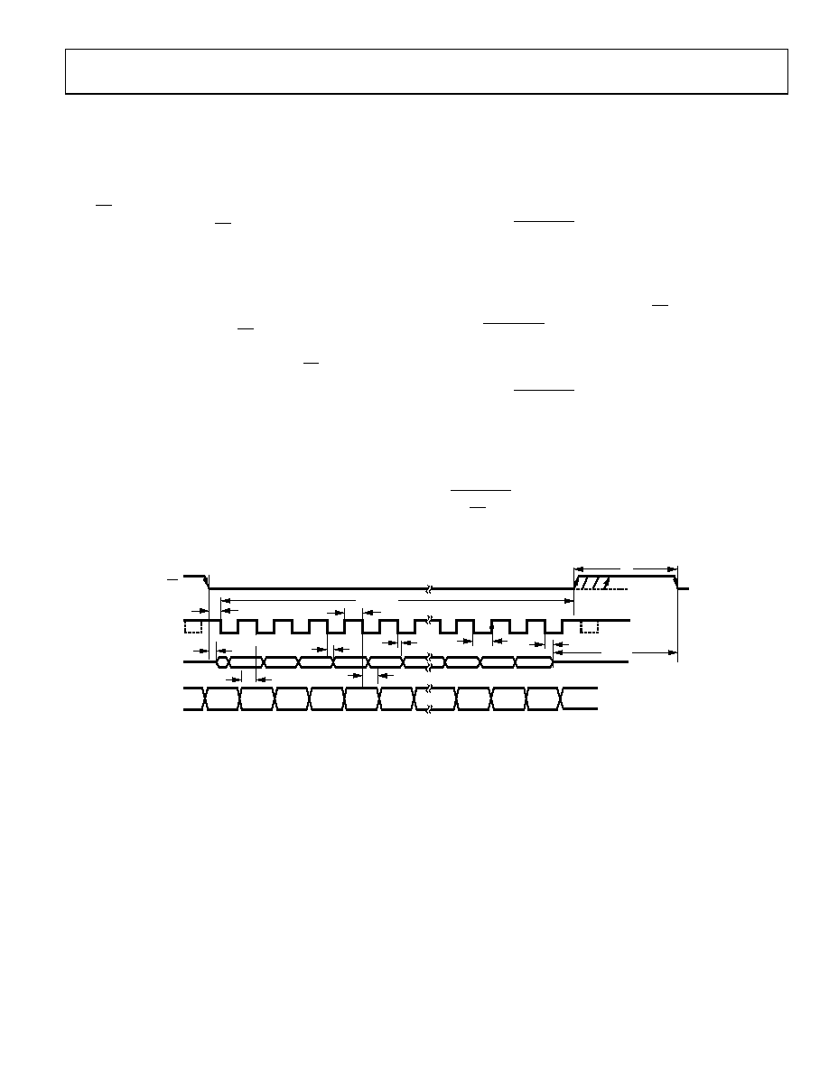
SERIAL INTERFACE
Figure 53 shows the timing diagram for the serial interface of
the AD7328. The serial clock applied to the SCLK pin provides
the conversion clock and controls the transfer of information to
and from the AD7328 during a conversion.
The CS signal initiates the data transfer and the conversion
process. The falling edge of CS puts the track-and-hold into
hold mode and takes the bus out of three-state. The analog
input signal is then sampled. After the conversion is initiated, 16
SCLK cycles are required for the conversion to complete.
The track-and-hold goes back into track mode on the 14th SCLK
rising edge. On the 16th SCLK falling edge, the DOUT line returns
to three-state. If the rising edge of CS occurs before 16 SCLK cycles
have elapsed, the conversion is terminated and the DOUT line
returns to three-state. Depending on where the CS signal is brought
high, the addressed register may update.
Data is clocked into the AD7328 on the SCLK falling edge. The
three MSBs on the DIN line are decoded to select which register
is addressed. The control register is a 12-bit register. If the control
register is addressed by the three MSBs, the data on the DIN line
is loaded into the control on the 15th SCLK rising edge. If the se-
quence register or either of the range registers is addressed, the
data on the DIN line is loaded into the addressed register on the
11th SCLK falling edge.
Conversion data is clocked out of the AD7328 on each SCLK
falling edge. Data on the DOUT line consists of three channel
identifier bits, a sign bit, and a 12-bit conversion result. The
channel identifier bits are used to indicate which channel
corresponds to the conversion result.
If the Weak/Three-State bit is set in the control register, rather
than returning to true three-state upon the 16th SCLK falling
edge, the DOUT line is pulled weakly to the logic level corres-
ponding to ADD3 of the next serial transfer. This is done to
ensure that the MSB of the next serial transfer is set up in time
for the first SCLK falling edge after the CS falling edge. If the
Weak/Three-State bit is set to 0 and the DOUT line returns to
true three-state between conversions, then depending on the
particular processor interfacing to the AD7328, the ADD3 bit
may be valid in time for the processor to clock it in successfully.
If the Weak/Three-State bit is set to 1, then although the DOUT
line has been driven to ADD3 since the previous conversion, it
is nevertheless so weakly driven that another device could take
control of the bus. This will not lead to a bus contention issue
because, for example, a 10 kΩ pull-up or pull-down resistor is
sufficient to overdrive the logic level of ADD3. When the Weak/
Three-State bit is set to 1, the ADD3 is typically valid 9 ns after
the CS falling edge, compared with 14 ns when the DOUT line
returns to three-state at the end of the conversion.
ADD1
1
2
3
4
5
13
14
15
16
WRITE
REG
SEL1
REG
SEL2
LSB
DON’T
CARE
MSB
ADD0
SIGN
DB11
DB10
DB2
DB1
DB0
t2
t6
t4
t9
t10
t3
t7
t5
t8
t1
tQUIET
tCONVERT
SCLK
CS
DOUT
THREE-
STATE
THREE-STATE
DIN
ADD2
3 IDENTIFICATION BITS
04852-
036
Figure 53. Serial Interface Timing Diagram (Control Register Write)
相关PDF资料 |
PDF描述 |
|---|---|
| AD7476AYKSZ-500RL7 | IC ADC 12BIT 1MSPS SC70-6 |
| NCS2200SN2T1G | IC COMPARATOR 1V LOW PWR 5TSOP |
| DS90CR218AMTD/NOPB | IC RCVR 21BIT CHAN LINK 48TSSOP |
| LTC2440IGN#PBF | IC ADC DIFFER 24-BIT HS 16-SSOP |
| VE-B1T-MX-F1 | CONVERTER MOD DC/DC 6.5V 75W |
相关代理商/技术参数 |
参数描述 |
|---|---|
| AD7328BRUZ | 制造商:Analog Devices 功能描述:A/D Converter (A-D) IC |
| AD7328BRUZ-REEL | 功能描述:IC ADC 12BIT+SAR 8CHAN 20-TSSOP RoHS:是 类别:集成电路 (IC) >> 数据采集 - 模数转换器 系列:iCMOS® 标准包装:1,000 系列:- 位数:16 采样率(每秒):45k 数据接口:串行 转换器数目:2 功率耗散(最大):315mW 电压电源:模拟和数字 工作温度:0°C ~ 70°C 安装类型:表面贴装 封装/外壳:28-SOIC(0.295",7.50mm 宽) 供应商设备封装:28-SOIC W 包装:带卷 (TR) 输入数目和类型:2 个单端,单极 |
| AD7328BRUZ-REEL7 | 功能描述:IC ADC 12BIT+ SAR 8CHAN 20TSSOP RoHS:是 类别:集成电路 (IC) >> 数据采集 - 模数转换器 系列:iCMOS® 标准包装:1,000 系列:- 位数:16 采样率(每秒):45k 数据接口:串行 转换器数目:2 功率耗散(最大):315mW 电压电源:模拟和数字 工作温度:0°C ~ 70°C 安装类型:表面贴装 封装/外壳:28-SOIC(0.295",7.50mm 宽) 供应商设备封装:28-SOIC W 包装:带卷 (TR) 输入数目和类型:2 个单端,单极 |
| AD7329 | 制造商:AD 制造商全称:Analog Devices 功能描述:1 MSPS, 8-Channel, Software-Selectable, True Bipolar Input, 12-Bit Plus Sign ADC |
| AD7329BRUZ | 功能描述:IC ADC 12BIT 8CH MUX SPI 24TSSOP RoHS:是 类别:集成电路 (IC) >> 数据采集 - 模数转换器 系列:- 标准包装:1 系列:microPOWER™ 位数:8 采样率(每秒):1M 数据接口:串行,SPI? 转换器数目:1 功率耗散(最大):- 电压电源:模拟和数字 工作温度:-40°C ~ 125°C 安装类型:表面贴装 封装/外壳:24-VFQFN 裸露焊盘 供应商设备封装:24-VQFN 裸露焊盘(4x4) 包装:Digi-Reel® 输入数目和类型:8 个单端,单极 产品目录页面:892 (CN2011-ZH PDF) 其它名称:296-25851-6 |
发布紧急采购,3分钟左右您将得到回复。