- 您现在的位置:买卖IC网 > PDF目录10672 > AD7328BRUZ (Analog Devices Inc)IC ADC 12BIT+ SAR 8CHAN 20TSSOP PDF资料下载
参数资料
| 型号: | AD7328BRUZ |
| 厂商: | Analog Devices Inc |
| 文件页数: | 35/37页 |
| 文件大小: | 0K |
| 描述: | IC ADC 12BIT+ SAR 8CHAN 20TSSOP |
| 设计资源: | Using AD7328 in Appls with Single-Ended Industrial-Level Signals (CN0047) |
| 标准包装: | 75 |
| 系列: | iCMOS® |
| 位数: | 12 |
| 采样率(每秒): | 1M |
| 数据接口: | DSP,MICROWIRE?,QSPI?,串行,SPI? |
| 转换器数目: | 1 |
| 功率耗散(最大): | 30mW |
| 电压电源: | 双 ± |
| 工作温度: | -40°C ~ 85°C |
| 安装类型: | 表面贴装 |
| 封装/外壳: | 20-TSSOP(0.173",4.40mm 宽) |
| 供应商设备封装: | 20-TSSOP |
| 包装: | 管件 |
| 输入数目和类型: | 8 个单端,单极;8 个单端,双极;4 个差分,单极;4 个差分,双极 |
| 产品目录页面: | 777 (CN2011-ZH PDF) |
第1页第2页第3页第4页第5页第6页第7页第8页第9页第10页第11页第12页第13页第14页第15页第16页第17页第18页第19页第20页第21页第22页第23页第24页第25页第26页第27页第28页第29页第30页第31页第32页第33页第34页当前第35页第36页第37页
AD7328
Data Sheet
Rev. C | Page 6 of 36
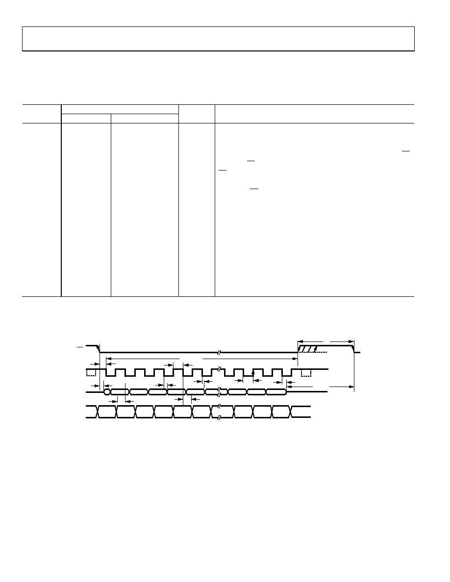
TIMING SPECIFICATIONS
VDD = 12 V to 16.5 V, VSS = 12 V to 16.5 V, VCC = 2.7 V to 5.25 V, VDRIVE = 2.7 V to 5.25 V, VREF = 2.5 V to 3.0 V internal/external,
Table 3.
Limit at TMIN, TMAX
Description
Parameter
VCC < 4.75 V
VCC = 4.75 V to 5.25 V
Unit
VDRIVE ≤ VCC
fSCLK
50
kHz min
14
20
MHz max
tCONVERT
16 × tSCLK
ns max
tSCLK = 1/fSCLK
tQUIET
75
60
ns min
Minimum time between end of serial read and next falling edge of CS
t1
12
5
ns min
Minimum CS pulse width
t22
25
20
ns min
CS to SCLK setup time; bipolar input ranges (±10 V, ±5 V, ±2.5 V)
45
35
ns min
Unipolar input range (0 V to 10 V)
t3
26
14
ns max
Delay from CS until DOUT three-state disabled
t4
57
43
ns max
Data access time after SCLK falling edge
t5
0.4 × tSCLK
ns min
SCLK low pulse width
t6
0.4 × tSCLK
ns min
SCLK high pulse width
t7
13
8
ns min
SCLK to data valid hold time
t8
40
22
ns max
SCLK falling edge to DOUT high impedance
10
9
ns min
SCLK falling edge to DOUT high impedance
t9
4
ns min
DIN setup time prior to SCLK falling edge
t10
2
ns min
DIN hold time after SCLK falling edge
tPOWER-UP
750
ns max
Power up from autostandby
500
s max
Power up from full shutdown/autoshutdown mode, internal reference
25
s typ
Power up from full shutdown/autoshutdown mode, external reference
1
Sample tested during initial release to ensure compliance. All input signals are specified with tr = tf = 5 ns (10% to 90% of VDRIVE) and timed from a voltage level of 1.6 V.
2
When using the 0 V to 10 V unipolar range, running at 1 MSPS throughput rate with t2 at 20 ns, the mark-space ratio must be limited to 50:50.
ADD1
1
2
3
4
5
13
14
15
16
WRITE
REG
SEL1
REG
SEL2
LSB
DON’T
CARE
MSB
ADD0
SIGN
DB11
DB10
DB2
DB1
DB0
t2
t6
t4
t9
t10
t3
t7
t5
t8
t1
tQUIET
tCONVERT
SCLK
CS
DOUT
THREE-
STATE
THREE-STATE
DIN
ADD2
3 IDENTIFICATION BITS
04852-
002
Figure 2. Serial Interface Timing Diagram
相关PDF资料 |
PDF描述 |
|---|---|
| AD7476AYKSZ-500RL7 | IC ADC 12BIT 1MSPS SC70-6 |
| NCS2200SN2T1G | IC COMPARATOR 1V LOW PWR 5TSOP |
| DS90CR218AMTD/NOPB | IC RCVR 21BIT CHAN LINK 48TSSOP |
| LTC2440IGN#PBF | IC ADC DIFFER 24-BIT HS 16-SSOP |
| VE-B1T-MX-F1 | CONVERTER MOD DC/DC 6.5V 75W |
相关代理商/技术参数 |
参数描述 |
|---|---|
| AD7328BRUZ | 制造商:Analog Devices 功能描述:A/D Converter (A-D) IC |
| AD7328BRUZ-REEL | 功能描述:IC ADC 12BIT+SAR 8CHAN 20-TSSOP RoHS:是 类别:集成电路 (IC) >> 数据采集 - 模数转换器 系列:iCMOS® 标准包装:1,000 系列:- 位数:16 采样率(每秒):45k 数据接口:串行 转换器数目:2 功率耗散(最大):315mW 电压电源:模拟和数字 工作温度:0°C ~ 70°C 安装类型:表面贴装 封装/外壳:28-SOIC(0.295",7.50mm 宽) 供应商设备封装:28-SOIC W 包装:带卷 (TR) 输入数目和类型:2 个单端,单极 |
| AD7328BRUZ-REEL7 | 功能描述:IC ADC 12BIT+ SAR 8CHAN 20TSSOP RoHS:是 类别:集成电路 (IC) >> 数据采集 - 模数转换器 系列:iCMOS® 标准包装:1,000 系列:- 位数:16 采样率(每秒):45k 数据接口:串行 转换器数目:2 功率耗散(最大):315mW 电压电源:模拟和数字 工作温度:0°C ~ 70°C 安装类型:表面贴装 封装/外壳:28-SOIC(0.295",7.50mm 宽) 供应商设备封装:28-SOIC W 包装:带卷 (TR) 输入数目和类型:2 个单端,单极 |
| AD7329 | 制造商:AD 制造商全称:Analog Devices 功能描述:1 MSPS, 8-Channel, Software-Selectable, True Bipolar Input, 12-Bit Plus Sign ADC |
| AD7329BRUZ | 功能描述:IC ADC 12BIT 8CH MUX SPI 24TSSOP RoHS:是 类别:集成电路 (IC) >> 数据采集 - 模数转换器 系列:- 标准包装:1 系列:microPOWER™ 位数:8 采样率(每秒):1M 数据接口:串行,SPI? 转换器数目:1 功率耗散(最大):- 电压电源:模拟和数字 工作温度:-40°C ~ 125°C 安装类型:表面贴装 封装/外壳:24-VFQFN 裸露焊盘 供应商设备封装:24-VQFN 裸露焊盘(4x4) 包装:Digi-Reel® 输入数目和类型:8 个单端,单极 产品目录页面:892 (CN2011-ZH PDF) 其它名称:296-25851-6 |
发布紧急采购,3分钟左右您将得到回复。