- 您现在的位置:买卖IC网 > PDF目录10543 > AD7366BRUZ-5 (Analog Devices Inc)IC ADC 12BIT DUAL 500KSPS 24-TSS PDF资料下载
参数资料
| 型号: | AD7366BRUZ-5 |
| 厂商: | Analog Devices Inc |
| 文件页数: | 15/28页 |
| 文件大小: | 0K |
| 描述: | IC ADC 12BIT DUAL 500KSPS 24-TSS |
| 设计资源: | Driving the AD7366/7 Bipolar SAR ADC in Low-Distortion DC-Coupled Appls (CN0042) |
| 标准包装: | 62 |
| 系列: | iCMOS® |
| 位数: | 12 |
| 采样率(每秒): | 500k |
| 数据接口: | DSP,MICROWIRE?,QSPI?,串行,SPI? |
| 转换器数目: | 2 |
| 功率耗散(最大): | 88.8mW |
| 电压电源: | 模拟和数字,双 ± |
| 工作温度: | -40°C ~ 85°C |
| 安装类型: | 表面贴装 |
| 封装/外壳: | 24-TSSOP(0.173",4.40mm 宽) |
| 供应商设备封装: | 24-TSSOP |
| 包装: | 管件 |
| 输入数目和类型: | 4 个单端,单极;4 个单端,双极 |
| 配用: | EVAL-AD7366CBZ-ND - BOARD EVALUATION FOR AD7366 |
第1页第2页第3页第4页第5页第6页第7页第8页第9页第10页第11页第12页第13页第14页当前第15页第16页第17页第18页第19页第20页第21页第22页第23页第24页第25页第26页第27页第28页
AD7366-5/AD7367-5
Rev. A | Page 22 of 28
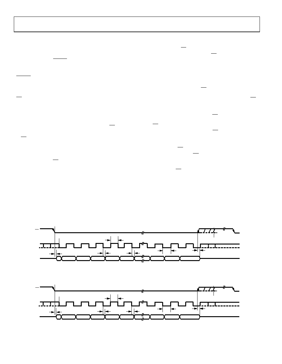
SERIAL INTERFACE
serial interfacing to the AD7366-5 and the AD7367-5, respectively.
On the falling edge of CNVST, the AD7366-5/AD7367-5 simulta-
neously converts the selected channels. These conversions are
performed using the on-chip oscillator. After the falling edge of
CNVST, the BUSY signal goes high, indicating the conversion has
started. It returns low once the conversion has been completed.
The data can now be read from the
DOUT pins.
CS and SCLK signals are required to transfer data from the
AD7366-5/AD7367-5. The parts have two output pins corre-
sponding to each ADC. Data can be read from the AD7366-5/
AD7367-5 using both DOUTA and DOUTB. Alternatively, a single
output pin of the user’s choice can be used. The SCLK input signal
provides the clock source for the serial interface. The CS goes
low to access data from the AD7366-5/AD7367-5. The falling edge
of CS takes the bus out of three-state and clocks out the MSB of
the conversion result. The data stream consists of 12 bits of data
for the AD7366-5 and 14 bits of data for the AD7367-5, MSB first.
The first bit of the conversion result is valid on the first SCLK
falling edge after the CS falling edge. The subsequent 11-bits/
13-bits of data for the AD7366-5/AD7367-5, respectively, are
clocked out on the falling edge of the SCLK signal. A minimum
of 12 clock pulses must be provided to the AD7366-5 to access
each conversion result, while a minimum of 14 clock pulses must
be provided to the AD7367-5 to access the conversion result.
Figure 25 shows how a 12 SCLK read is used to access the
conversion results, while Figure 26 illustrates the case for the
AD7367-5 with a 14 SCLK read.
On the rising edge of CS, the conversion is terminated, and DOUTA
and DOUTB go back into three-state. If CS is not brought high,
but is instead held low for a further 12 SCLK cycles for the
AD7366-5 or 14 SCLK cycles for the AD7367-5 on either DOUTA
or DOUTB, the data from the other ADC follows on that DOUT pin.
This is illustrated in
and
where the case for
DOUTA is shown. In this case, the DOUT line in use goes back into
three-state on the rising edge of
CS.
If the falling edge of SCLK coincides with the falling edge of CS,
the falling edge of SCLK is not acknowledged by the AD7366-5/
AD7367-5, and the next falling edge of the SCLK is the first
registered after the falling edges of the CS.
The CS pin can be brought low before the BUSY signal goes low,
indicating the end of a conversion. Once CS is at a logic low state,
the data bus is brought out of three-state. This feature can be
utilized to ensure that the MSB is valid on the falling edge of
BUSY by bringing CS low a minimum of t4 ns before the BUSY
signal goes low. The dotted CS
line in
and
illustrates this.
Alternatively, the CS pin can be tied to a low logic state continu-
ously. In this case, the DOUT pins never enter three-state, and the
data bus is continuously active. Under these conditions, the MSB
of the conversion result for the AD7366-5/AD7367-5 is available
on the falling edge of the BUSY signal. The next most significant
bit is available on the first SCLK falling edge after the BUSY
signal has gone low. This mode of operation enables the user to
read the MSB as soon as it is made available by the converter.
DOUTA
DOUTB THREE-
STATE
THREE-STATE
CS
SCLK
1
512
2
34
DB10
DB11
DB9
DB8
DB2
DB1
DB0
t5
t6
t8
t4
t9
t7
06
84
2
-02
7
DOUTA
DOUTB THREE-
STATE
THREE-STATE
Figure 25. Serial Interface Timing Diagram for the AD7366-5
CS
SCLK
1
514
2
34
DB12
DB13
DB11
DB10
DB2
DB1
DB0
t5
t6
t8
t4
t9
t7
0
68
42
-02
8
Figure 26. Serial Interface Timing Diagram for the AD7367-5
相关PDF资料 |
PDF描述 |
|---|---|
| VI-B51-IV-F2 | CONVERTER MOD DC/DC 12V 150W |
| AD7475BRMZ | IC ADC 12BIT SERIAL LP 8MSOP |
| ISL3295EIHZ-T7A | IC TXRX |
| AD9215BCPZ-65 | IC ADC 10BIT 65MSPS 32-LFCSP |
| AD7898ARZ-3 | IC ADC 12BIT SRL HS 5V 8SOIC |
相关代理商/技术参数 |
参数描述 |
|---|---|
| AD7366BRUZ-500RL7 | 功能描述:IC ADC 12BIT SAR 1MSPS 24TSSOP RoHS:是 类别:集成电路 (IC) >> 数据采集 - 模数转换器 系列:iCMOS® 标准包装:1,000 系列:- 位数:16 采样率(每秒):45k 数据接口:串行 转换器数目:2 功率耗散(最大):315mW 电压电源:模拟和数字 工作温度:0°C ~ 70°C 安装类型:表面贴装 封装/外壳:28-SOIC(0.295",7.50mm 宽) 供应商设备封装:28-SOIC W 包装:带卷 (TR) 输入数目和类型:2 个单端,单极 |
| AD7366BRUZ-5500RL7 | 功能描述:IC ADC 12BIT DUAL BIPO 24-TSSOP RoHS:是 类别:集成电路 (IC) >> 数据采集 - 模数转换器 系列:iCMOS® 标准包装:1,000 系列:- 位数:16 采样率(每秒):45k 数据接口:串行 转换器数目:2 功率耗散(最大):315mW 电压电源:模拟和数字 工作温度:0°C ~ 70°C 安装类型:表面贴装 封装/外壳:28-SOIC(0.295",7.50mm 宽) 供应商设备封装:28-SOIC W 包装:带卷 (TR) 输入数目和类型:2 个单端,单极 |
| AD7366BRUZ-5-RL7 | 功能描述:IC ADC 12BIT DUAL BIPO 24-TSSOP RoHS:是 类别:集成电路 (IC) >> 数据采集 - 模数转换器 系列:iCMOS® 标准包装:1,000 系列:- 位数:16 采样率(每秒):45k 数据接口:串行 转换器数目:2 功率耗散(最大):315mW 电压电源:模拟和数字 工作温度:0°C ~ 70°C 安装类型:表面贴装 封装/外壳:28-SOIC(0.295",7.50mm 宽) 供应商设备封装:28-SOIC W 包装:带卷 (TR) 输入数目和类型:2 个单端,单极 |
| AD7366BRUZ-REEL7 | 制造商:AD 制造商全称:Analog Devices 功能描述:True Bipolar Input, Dual 1us, 12-Bit, 2-Channel SAR ADC |
| AD7366BRUZ-RL7 | 功能描述:IC ADC 12BIT SAR 1MSPS 24TSSOP RoHS:是 类别:集成电路 (IC) >> 数据采集 - 模数转换器 系列:iCMOS® 标准包装:1,000 系列:- 位数:16 采样率(每秒):45k 数据接口:串行 转换器数目:2 功率耗散(最大):315mW 电压电源:模拟和数字 工作温度:0°C ~ 70°C 安装类型:表面贴装 封装/外壳:28-SOIC(0.295",7.50mm 宽) 供应商设备封装:28-SOIC W 包装:带卷 (TR) 输入数目和类型:2 个单端,单极 |
发布紧急采购,3分钟左右您将得到回复。