- 您现在的位置:买卖IC网 > PDF目录10543 > AD7366BRUZ-5 (Analog Devices Inc)IC ADC 12BIT DUAL 500KSPS 24-TSS PDF资料下载
参数资料
| 型号: | AD7366BRUZ-5 |
| 厂商: | Analog Devices Inc |
| 文件页数: | 8/28页 |
| 文件大小: | 0K |
| 描述: | IC ADC 12BIT DUAL 500KSPS 24-TSS |
| 设计资源: | Driving the AD7366/7 Bipolar SAR ADC in Low-Distortion DC-Coupled Appls (CN0042) |
| 标准包装: | 62 |
| 系列: | iCMOS® |
| 位数: | 12 |
| 采样率(每秒): | 500k |
| 数据接口: | DSP,MICROWIRE?,QSPI?,串行,SPI? |
| 转换器数目: | 2 |
| 功率耗散(最大): | 88.8mW |
| 电压电源: | 模拟和数字,双 ± |
| 工作温度: | -40°C ~ 85°C |
| 安装类型: | 表面贴装 |
| 封装/外壳: | 24-TSSOP(0.173",4.40mm 宽) |
| 供应商设备封装: | 24-TSSOP |
| 包装: | 管件 |
| 输入数目和类型: | 4 个单端,单极;4 个单端,双极 |
| 配用: | EVAL-AD7366CBZ-ND - BOARD EVALUATION FOR AD7366 |
第1页第2页第3页第4页第5页第6页第7页当前第8页第9页第10页第11页第12页第13页第14页第15页第16页第17页第18页第19页第20页第21页第22页第23页第24页第25页第26页第27页第28页
AD7366-5/AD7367-5
Rev. A | Page 16 of 28
THEORY OF OPERATION
CIRCUIT INFORMATION
The AD7366-5/AD7367-5 are fast, dual, 2-channel, 12-/14-bit,
bipolar input, simultaneous sampling, serial ADCs. The
AD7366-5/AD7367-5 can accept bipolar input ranges of ±10 V
and ±5 V. They can also accept a 0 V to 10 V unipolar input
range. The AD7366-5/AD7367-5 require VDD and VSS dual
supplies for the high voltage analog input structure. These
supplies must be greater than or equal to the analog input range
(see Table 7 for the minimum requirements on these supplies
for each analog input range). The AD7366-5/AD7367-5 require
a low voltage 4.75 V to 5.25 V VCC supply to power the ADC core.
Table 7. Reference and Supply Requirements for Each
Analog Input Range
Selected
Analog Input
Range (V)
Reference
Voltage (V)
Full-Scale
Input
Range (V)
AVCC (V)
Minimum
VDD/VSS (V)
±10
+2.5
±10
+5
±10
+3.0
±12
+5
±12
±5
+2.5
±5
+5
±5
+3.0
±6
+5
±6
0 to +10
+2.5
0 to +10
+5
+10/AGND
+3.0
0 to +12
+5
+12/AGND
Each AD7366-5/AD7367-5 contains two on-chip, track-and-hold
amplifiers, two successive approximation ADCs, and a serial
interface with two separate data output pins. The device is housed
in a 24-lead TSSOP, offering the user considerable space-saving
advantages over alternative solutions.
The AD7366-5/AD7367-5 require a CNVST signal to start a
conversion. On the falling edge of CNVST, both track-and-
holds are placed into hold mode, and the conversions are
initiated. The BUSY signal goes high to indicate that the
conversions are taking place. The clock source for each
successive approximation ADC is provided by an internal
oscillator. The BUSY signal goes low to indicate the end of
conversion. On the falling edge of BUSY, the track-and-hold
returns to track mode. Once the conversion is finished, the
serial clock input accesses data from the part.
The AD7366-5/AD7367-5 have an on-chip 2.5 V reference that
can be disabled when an external reference is preferred. If the
internal reference is to be used elsewhere in a system, the output
from DCAPA and DCAPB must first be buffered. On power-up, the
REFSEL pin must be tied to a high or low logic state to select
either the internal or external reference option.
If the internal reference is the preferred option, the user must
tie the REFSEL pin logic high. Alternatively, if REFSEL is tied to
GND, an external reference can be supplied to both ADCs
through the DCAPA and DCAPB pins.
The analog inputs are configured as two single-ended inputs for
each ADC. The various different input voltage ranges can be
selected by programming the RANGE bits as shown in Table 8.
CONVERTER OPERATION
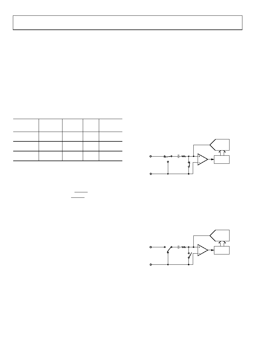
The AD7366-5/AD7367-5 have two successive approximation
ADCs, each based around two capacitive DACs. Figure 16 and
Figure 17 show simplified schematics of an ADC in acquisition
and conversion phases, respectively. The ADC is comprised of
control logic, a SAR, and a capacitive DAC. In Figure 16 (the
acquisition phase), SW2 is closed, SW1 is in Position A, the
comparator is held in a balanced condition, and the sampling
capacitor arrays acquire the signal on the input.
CAPACITIVE
DAC
CONTROL
LOGIC
VIN
AGND
A
B
SW1
SW2
COMPARATOR
68
42-
0
18
0
Figure 16. ADC Acquisition Phase
When the ADC starts a conversion (see Figure 17), SW2 opens,
and SW1 moves to Position B, causing the comparator to
become unbalanced. The control logic and the charge redis-
tribution DAC is used to add and subtract fixed amounts of
charge from the sampling capacitor to bring the comparator
back into a balanced condition. When the comparator is
balanced again, the conversion is complete. The control logic
generates the ADC output code.
CAPACITIVE
DAC
CONTROL
LOGIC
VIN
AGND
A
B
SW1
SW2
COMPARATOR
0
68
42
-01
9
Figure 17. ADC Conversion Phase
相关PDF资料 |
PDF描述 |
|---|---|
| VI-B51-IV-F2 | CONVERTER MOD DC/DC 12V 150W |
| AD7475BRMZ | IC ADC 12BIT SERIAL LP 8MSOP |
| ISL3295EIHZ-T7A | IC TXRX |
| AD9215BCPZ-65 | IC ADC 10BIT 65MSPS 32-LFCSP |
| AD7898ARZ-3 | IC ADC 12BIT SRL HS 5V 8SOIC |
相关代理商/技术参数 |
参数描述 |
|---|---|
| AD7366BRUZ-500RL7 | 功能描述:IC ADC 12BIT SAR 1MSPS 24TSSOP RoHS:是 类别:集成电路 (IC) >> 数据采集 - 模数转换器 系列:iCMOS® 标准包装:1,000 系列:- 位数:16 采样率(每秒):45k 数据接口:串行 转换器数目:2 功率耗散(最大):315mW 电压电源:模拟和数字 工作温度:0°C ~ 70°C 安装类型:表面贴装 封装/外壳:28-SOIC(0.295",7.50mm 宽) 供应商设备封装:28-SOIC W 包装:带卷 (TR) 输入数目和类型:2 个单端,单极 |
| AD7366BRUZ-5500RL7 | 功能描述:IC ADC 12BIT DUAL BIPO 24-TSSOP RoHS:是 类别:集成电路 (IC) >> 数据采集 - 模数转换器 系列:iCMOS® 标准包装:1,000 系列:- 位数:16 采样率(每秒):45k 数据接口:串行 转换器数目:2 功率耗散(最大):315mW 电压电源:模拟和数字 工作温度:0°C ~ 70°C 安装类型:表面贴装 封装/外壳:28-SOIC(0.295",7.50mm 宽) 供应商设备封装:28-SOIC W 包装:带卷 (TR) 输入数目和类型:2 个单端,单极 |
| AD7366BRUZ-5-RL7 | 功能描述:IC ADC 12BIT DUAL BIPO 24-TSSOP RoHS:是 类别:集成电路 (IC) >> 数据采集 - 模数转换器 系列:iCMOS® 标准包装:1,000 系列:- 位数:16 采样率(每秒):45k 数据接口:串行 转换器数目:2 功率耗散(最大):315mW 电压电源:模拟和数字 工作温度:0°C ~ 70°C 安装类型:表面贴装 封装/外壳:28-SOIC(0.295",7.50mm 宽) 供应商设备封装:28-SOIC W 包装:带卷 (TR) 输入数目和类型:2 个单端,单极 |
| AD7366BRUZ-REEL7 | 制造商:AD 制造商全称:Analog Devices 功能描述:True Bipolar Input, Dual 1us, 12-Bit, 2-Channel SAR ADC |
| AD7366BRUZ-RL7 | 功能描述:IC ADC 12BIT SAR 1MSPS 24TSSOP RoHS:是 类别:集成电路 (IC) >> 数据采集 - 模数转换器 系列:iCMOS® 标准包装:1,000 系列:- 位数:16 采样率(每秒):45k 数据接口:串行 转换器数目:2 功率耗散(最大):315mW 电压电源:模拟和数字 工作温度:0°C ~ 70°C 安装类型:表面贴装 封装/外壳:28-SOIC(0.295",7.50mm 宽) 供应商设备封装:28-SOIC W 包装:带卷 (TR) 输入数目和类型:2 个单端,单极 |
发布紧急采购,3分钟左右您将得到回复。