- 您现在的位置:买卖IC网 > PDF目录10543 > AD7366BRUZ-5 (Analog Devices Inc)IC ADC 12BIT DUAL 500KSPS 24-TSS PDF资料下载
参数资料
| 型号: | AD7366BRUZ-5 |
| 厂商: | Analog Devices Inc |
| 文件页数: | 28/28页 |
| 文件大小: | 0K |
| 描述: | IC ADC 12BIT DUAL 500KSPS 24-TSS |
| 设计资源: | Driving the AD7366/7 Bipolar SAR ADC in Low-Distortion DC-Coupled Appls (CN0042) |
| 标准包装: | 62 |
| 系列: | iCMOS® |
| 位数: | 12 |
| 采样率(每秒): | 500k |
| 数据接口: | DSP,MICROWIRE?,QSPI?,串行,SPI? |
| 转换器数目: | 2 |
| 功率耗散(最大): | 88.8mW |
| 电压电源: | 模拟和数字,双 ± |
| 工作温度: | -40°C ~ 85°C |
| 安装类型: | 表面贴装 |
| 封装/外壳: | 24-TSSOP(0.173",4.40mm 宽) |
| 供应商设备封装: | 24-TSSOP |
| 包装: | 管件 |
| 输入数目和类型: | 4 个单端,单极;4 个单端,双极 |
| 配用: | EVAL-AD7366CBZ-ND - BOARD EVALUATION FOR AD7366 |
第1页第2页第3页第4页第5页第6页第7页第8页第9页第10页第11页第12页第13页第14页第15页第16页第17页第18页第19页第20页第21页第22页第23页第24页第25页第26页第27页当前第28页
AD7366-5/AD7367-5
Rev. A | Page 9 of 28
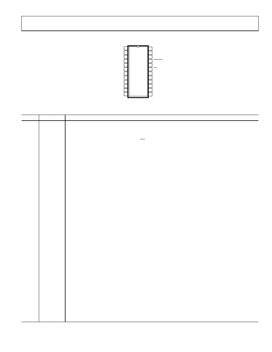
PIN CONFIGURATION AND FUNCTION DESCRIPTIONS
DOUTA 1
2
3
ADDR
4
DGND
24
23
BUSY
22
CNVST
21
RANGE0 5
RANGE1
6
AGND 7
SCLK
20
CS
19
REFSEL
18
8
AGND
17
9
16
10
15
11
14
12
13
AD7366-5/
AD7367-5
TOP VIEW
(Not to Scale)
DOUTB
DCAPADCAPB
DVCC
AVCC
VSS
VDD
VDRIVE
VA1
VA2
VB1
VB2
06
84
2-
00
2
Figure 2. Pin Configuration
Table 6. Pin Function Descriptions
Pin No.
Mnemonic
Description
1, 23
DOUTA, DOUTB
Serial Data Outputs. The data output is supplied to each pin as a serial data stream. The bits are clocked out on
the falling edge of the SCLK input and 12 SCLK cycles are required to access the data from the AD7366-5 while
14 SCLK cycle are required for the AD7367-5. The data simultaneously appears on both pins from the simultaneous
conversions of both ADCs. The data stream consists of the 12 bits of conversion data for the AD7366-5 and 14 bits
for the AD7367-5 and is provided MSB first. If CS is held low for a further 12 SCLK cycles for the AD7366-5 or 14 SCLK
cycles for the AD7367-5, on either DOUTA or DOUTB, the data from the other ADC follows on that DOUT pin. This
allows data from a simultaneous conversion on both ADCs to be gathered in serial format on either DOUTA or
DOUTB using only one serial port. See the
section for more information.
2
VDRIVE
Logic Power Supply Input. The voltage supplied at this pin determines at what voltage the interface operates.
This pin should be decoupled to DGND. The voltage range on this pin is 2.7 V to 5.25 V and may be different than
the voltage at AVCC and DVCC, but should never exceed either by more than 0.3 V.
3
DVCC
Digital Supply Voltage, 4.75 V to 5.25 V. The DVCC and AVCC voltages should ideally be at the same potential.
For best performance, it is recommended that the DVCC and AVCC pins be shorted together, to ensure that the
voltage difference between them never exceeds 0.3 V, even on a transient basis. This supply should be decoupled
to DGND. Place 10 μF and 100 nF decoupling capacitors on the DVCC pin.
4, 5
RANGE1,
RANGE0
Analog Input Range Selection, Logic Inputs. The polarity on these pins determines the input range of the analog
input channels. See the Analog Inputs section and Table 8 for details.
6
ADDR
Multiplexer Select, Logic Input. This input is used to select the pair of channels to be simultaneously converted,
either Channel 1 of both ADC A and ADC B, or Channel 2 of both ADC A and ADC B. The logic state on this pin is
latched on the rising edge of BUSY to set up the multiplexer for the next conversion.
7, 17
AGND
Analog Ground. Ground reference point for all analog circuitry on the AD7366-5/AD7367-5. All analog input
signals and any external reference signal should be referred to this AGND voltage. Both AGND pins should
connect to the AGND plane of a system. The AGND and DGND voltages ideally should be at the same potential
and must not be more than 0.3 V apart, even on a transient basis.
8
AVCC
Analog Supply Voltage, 4.75 V to 5.25 V. This is the supply voltage for the ADC cores. The AVCC and DVCC voltages
should ideally be at the same potential. For best performance, it is recommended that the DVCC and AVCC pins be
shorted together to ensure that the voltage difference between them never exceeds 0.3 V even on a transient
basis. This supply should be decoupled to AGND. Place 10 μF and 100 nF decoupling capacitors on the AVCC pin.
9, 16
DCAPA, DCAPB
Decoupling Capacitor Pins. Decoupling capacitors are connected to these pins to decouple the reference buffer
for each respective ADC. For best performance, it is recommended to use a 680 nF decoupling capacitor on these
pins. Provided the output is buffered, the on-chip reference can be taken from these pins and applied externally
to the rest of a system.
10
VSS
Negative Power Supply Voltage. This is the negative supply voltage for the high voltage analog input structure
of the AD7366-5/AD7367-5. The supply must be less than or equal to 5 V (see Table 7 for further details).
Place 10 μF and 100 nF decoupling capacitors on the VSS pin.
11, 12
VA1, VA2
Analog Inputs of ADC A. These are both single-ended analog inputs. The analog input range on these channels is
determined by the RANGE0 and RANGE1 pins.
13, 14
VB2, VB1
Analog Inputs of ADC B. These are both single-ended analog inputs. The analog input range on these channels is
determined by the RANGE0 and RANGE1 pins.
15
VDD
Positive Power Supply Voltage. This is the positive supply voltage for the high voltage analog input structure
of the AD7366-5/AD7367-5. The supply must be greater than or equal to 5 V (see Table 7 for further details).
Place 10 μF and 100 nF decoupling capacitors on the VDD pin.
相关PDF资料 |
PDF描述 |
|---|---|
| VI-B51-IV-F2 | CONVERTER MOD DC/DC 12V 150W |
| AD7475BRMZ | IC ADC 12BIT SERIAL LP 8MSOP |
| ISL3295EIHZ-T7A | IC TXRX |
| AD9215BCPZ-65 | IC ADC 10BIT 65MSPS 32-LFCSP |
| AD7898ARZ-3 | IC ADC 12BIT SRL HS 5V 8SOIC |
相关代理商/技术参数 |
参数描述 |
|---|---|
| AD7366BRUZ-500RL7 | 功能描述:IC ADC 12BIT SAR 1MSPS 24TSSOP RoHS:是 类别:集成电路 (IC) >> 数据采集 - 模数转换器 系列:iCMOS® 标准包装:1,000 系列:- 位数:16 采样率(每秒):45k 数据接口:串行 转换器数目:2 功率耗散(最大):315mW 电压电源:模拟和数字 工作温度:0°C ~ 70°C 安装类型:表面贴装 封装/外壳:28-SOIC(0.295",7.50mm 宽) 供应商设备封装:28-SOIC W 包装:带卷 (TR) 输入数目和类型:2 个单端,单极 |
| AD7366BRUZ-5500RL7 | 功能描述:IC ADC 12BIT DUAL BIPO 24-TSSOP RoHS:是 类别:集成电路 (IC) >> 数据采集 - 模数转换器 系列:iCMOS® 标准包装:1,000 系列:- 位数:16 采样率(每秒):45k 数据接口:串行 转换器数目:2 功率耗散(最大):315mW 电压电源:模拟和数字 工作温度:0°C ~ 70°C 安装类型:表面贴装 封装/外壳:28-SOIC(0.295",7.50mm 宽) 供应商设备封装:28-SOIC W 包装:带卷 (TR) 输入数目和类型:2 个单端,单极 |
| AD7366BRUZ-5-RL7 | 功能描述:IC ADC 12BIT DUAL BIPO 24-TSSOP RoHS:是 类别:集成电路 (IC) >> 数据采集 - 模数转换器 系列:iCMOS® 标准包装:1,000 系列:- 位数:16 采样率(每秒):45k 数据接口:串行 转换器数目:2 功率耗散(最大):315mW 电压电源:模拟和数字 工作温度:0°C ~ 70°C 安装类型:表面贴装 封装/外壳:28-SOIC(0.295",7.50mm 宽) 供应商设备封装:28-SOIC W 包装:带卷 (TR) 输入数目和类型:2 个单端,单极 |
| AD7366BRUZ-REEL7 | 制造商:AD 制造商全称:Analog Devices 功能描述:True Bipolar Input, Dual 1us, 12-Bit, 2-Channel SAR ADC |
| AD7366BRUZ-RL7 | 功能描述:IC ADC 12BIT SAR 1MSPS 24TSSOP RoHS:是 类别:集成电路 (IC) >> 数据采集 - 模数转换器 系列:iCMOS® 标准包装:1,000 系列:- 位数:16 采样率(每秒):45k 数据接口:串行 转换器数目:2 功率耗散(最大):315mW 电压电源:模拟和数字 工作温度:0°C ~ 70°C 安装类型:表面贴装 封装/外壳:28-SOIC(0.295",7.50mm 宽) 供应商设备封装:28-SOIC W 包装:带卷 (TR) 输入数目和类型:2 个单端,单极 |
发布紧急采购,3分钟左右您将得到回复。