- 您现在的位置:买卖IC网 > PDF目录10571 > AD7452BRTZ-R2 (Analog Devices Inc)IC ADC 12BIT 555KSPS SOT23-8 PDF资料下载
参数资料
| 型号: | AD7452BRTZ-R2 |
| 厂商: | Analog Devices Inc |
| 文件页数: | 11/29页 |
| 文件大小: | 0K |
| 描述: | IC ADC 12BIT 555KSPS SOT23-8 |
| 标准包装: | 1 |
| 位数: | 12 |
| 采样率(每秒): | 555k |
| 数据接口: | DSP,MICROWIRE?,QSPI?,串行,SPI? |
| 转换器数目: | 1 |
| 功率耗散(最大): | 7.25mW |
| 电压电源: | 单电源 |
| 工作温度: | -40°C ~ 85°C |
| 安装类型: | 表面贴装 |
| 封装/外壳: | SOT-23-8 |
| 供应商设备封装: | SOT-23-8 |
| 包装: | 标准包装 |
| 输入数目和类型: | 1 个差分,双极 |
| 产品目录页面: | 777 (CN2011-ZH PDF) |
| 其它名称: | AD7452BRTZ-R2DKR |
第1页第2页第3页第4页第5页第6页第7页第8页第9页第10页当前第11页第12页第13页第14页第15页第16页第17页第18页第19页第20页第21页第22页第23页第24页第25页第26页第27页第28页第29页
AD7452
Rev. B | Page 18 of 28
DIGITAL INPUTS
The digital inputs applied to the AD7452 are not limited by the
maximum ratings, which limit the analog limits. Instead the
digital inputs applied, i.e., CS and SCLK, can go to 7 V and are
not restricted by the VDD + 0.3 V limits as on the analog input.
The main advantage of the inputs being unrestricted to the
VDD + 0.3 V limit is that power supply sequencing issues are
avoided. If CS and SCLK are applied before VDD, there is no risk
of latch-up as there would be on the analog inputs if a signal
greater than 0.3 V was applied prior to VDD.
REFERENCE
An external reference source is required to supply the reference
to the AD7452. This reference input can range from 100 mV to
3.5 V. With a 5 V power supply, the specified reference is 2.5 V
and the maximum reference is 3.5 V. With a 3 V power supply,
the specified reference is 2 V and the maximum reference is
2.2 V. In both cases, the reference is functional from 100 mV.
It is important to ensure that when choosing the reference value
for a particular application, the maximum analog input range
(VIN max) is never greater than VDD + 0.3 V to comply with the
maximum ratings of the device. The following two examples
calculate the maximum VREF input that can be used when
operating the AD7452 at a VDD of 5 V and 3 V, respectively.
Example 1
VIN max = VDD + 0.3
VIN max = VREF + VREF/2
If VDD = 5 V, then VIN max = 5.3 V.
Therefore
3 × VREF/2 = 5.3 V
VREF max = 3.5 V
Thus, when operating at VDD = 5 V, the value of VREF can range
from 100 mV to a maximum value of 3.5 V. When VDD = 4.75 V,
VREF max = 3.17 V.
Example 2
VIN max = VDD + 0.3
VIN max = VREF + VREF/2
If VDD = 3 V, then VIN max = 3.3 V.
Therefore
3 × VREF/2 = 3.3 V
VREF max = 2.2 V
Thus, when operating at VDD = 3 V, the value of VREF can range
from 100 mV to a maximum value of 2.2 V. When VDD = 2.7 V,
VREF max = 2 V.
These examples show that the maximum reference applied to
the AD7452 is directly dependent on the value applied to VDD.
The value of the reference sets the analog input span and the
common-mode voltage range. Errors in the reference source
result in gain errors in the AD7452 transfer function and add to
specified full-scale errors on the part. A 0.1 F capacitor should
be used to decouple the VREF pin to GND.
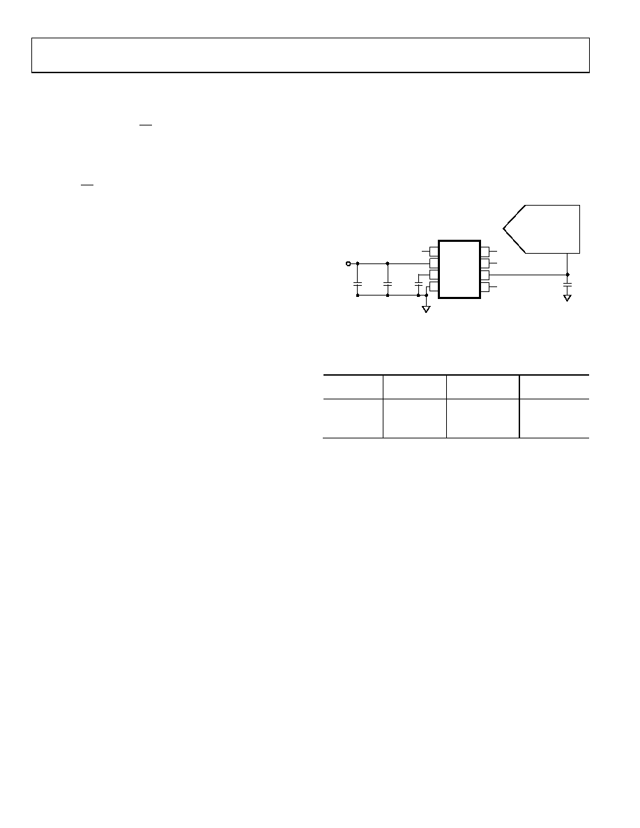
1
AD780
NC
8
2
VIN
NC
7
3
GND
6
4
TEMP
5
OPSEL
TRIM
VOUT
AD7452*
VREF
2.5V
NC
VDD
NC
VDD
NC = NO CONNECT
10nF
0.1
F
0.1
F
0.1
F
03154-A
-033
*ADDITIONAL PINS OMITTED FOR CLARITY
Figure 33. Typical VREF Connection Diagram for VDD = 5 V
Table 5. Examples of Suitable Voltage References
Reference
Output
Voltage (V)
Initial
Accuracy (%)
Operating
Current (A)
AD780
2.5/3
0.04
1000
ADR421
2.5
0.04
500
ADR420
2.048
0.05
500
SINGLE-ENDED OPERATION
When supplied with a 5 V power supply, the AD7452 can han-
dle a single-ended input. The design of this part is optimized for
differential operation, so with a single-ended input, perfor-
mance degrades. Linearity degrades by 0.2 LSB typically, the
full-scale errors degrade by 1 LSB typically, and ac performance
is not guaranteed.
To operate the AD7452 in single-ended mode, the VIN+ input is
coupled to the signal source, while the VIN– input is biased to the
appropriate voltage corresponding to the midscale code transi-
tion. This voltage is the common mode, which is a fixed dc
voltage (usually the reference). The VIN+ input swings around
this value and should have a voltage span of 2 × VREF to make
use of the full dynamic range of the part. The input signal
therefore has peak-to-peak values of common mode ± VREF. If
the analog input is unipolar, an op amp in a noninverting unity
gain configuration can be used to drive the VIN+ pin. Because
the ADC operates from a single supply, it is necessary to level
shift ground-based bipolar signals to comply with the input
requirements. An op amp can be configured to rescale and level
shift the ground-based bipolar signal so it is compatible with
the selected input range of the AD7452 (see Figure 34).
相关PDF资料 |
PDF描述 |
|---|---|
| PX0921/04/S | CONN RCPT 4POS W/SOCKET |
| VE-JT4-MW-F3 | CONVERTER MOD DC/DC 48V 100W |
| SP3245ECY-L | IC TXRX RS233 28TSSOP |
| VE-JVY-MY-F4 | CONVERTER MOD DC/DC 3.3V 33W |
| VE-JT4-MW-F1 | CONVERTER MOD DC/DC 48V 100W |
相关代理商/技术参数 |
参数描述 |
|---|---|
| AD7452BRTZ-REEL7 | 功能描述:IC ADC 12BIT DIF 555KSPS SOT23-8 RoHS:是 类别:集成电路 (IC) >> 数据采集 - 模数转换器 系列:- 标准包装:2,500 系列:- 位数:16 采样率(每秒):15 数据接口:MICROWIRE?,串行,SPI? 转换器数目:1 功率耗散(最大):480µW 电压电源:单电源 工作温度:-40°C ~ 85°C 安装类型:表面贴装 封装/外壳:38-WFQFN 裸露焊盘 供应商设备封装:38-QFN(5x7) 包装:带卷 (TR) 输入数目和类型:16 个单端,双极;8 个差分,双极 配用:DC1011A-C-ND - BOARD DELTA SIGMA ADC LTC2494 |
| AD7453 | 制造商:AD 制造商全称:Analog Devices 功能描述:Pseudo Differential, 555 kSPS, 12-Bit ADC in an 8-Lead SOT-23 |
| AD7453ART-REEL7 | 制造商:Analog Devices 功能描述: |
| AD7453ARTZ-REEL7 | 功能描述:IC ADC 12BIT DFF 600KSPS SOT23-8 RoHS:是 类别:集成电路 (IC) >> 数据采集 - 模数转换器 系列:- 标准包装:2,500 系列:- 位数:16 采样率(每秒):15 数据接口:MICROWIRE?,串行,SPI? 转换器数目:1 功率耗散(最大):480µW 电压电源:单电源 工作温度:-40°C ~ 85°C 安装类型:表面贴装 封装/外壳:38-WFQFN 裸露焊盘 供应商设备封装:38-QFN(5x7) 包装:带卷 (TR) 输入数目和类型:16 个单端,双极;8 个差分,双极 配用:DC1011A-C-ND - BOARD DELTA SIGMA ADC LTC2494 |
| AD7453BRT-R2 | 制造商:Analog Devices 功能描述:ADC Single SAR 555ksps 12-bit Serial 8-Pin SOT-23 T/R 制造商:Rochester Electronics LLC 功能描述:12-BIT P/DIFF I/PUT, 600KSPS ADC I.C. - Bulk |
发布紧急采购,3分钟左右您将得到回复。