- 您现在的位置:买卖IC网 > PDF目录10571 > AD7452BRTZ-R2 (Analog Devices Inc)IC ADC 12BIT 555KSPS SOT23-8 PDF资料下载
参数资料
| 型号: | AD7452BRTZ-R2 |
| 厂商: | Analog Devices Inc |
| 文件页数: | 14/29页 |
| 文件大小: | 0K |
| 描述: | IC ADC 12BIT 555KSPS SOT23-8 |
| 标准包装: | 1 |
| 位数: | 12 |
| 采样率(每秒): | 555k |
| 数据接口: | DSP,MICROWIRE?,QSPI?,串行,SPI? |
| 转换器数目: | 1 |
| 功率耗散(最大): | 7.25mW |
| 电压电源: | 单电源 |
| 工作温度: | -40°C ~ 85°C |
| 安装类型: | 表面贴装 |
| 封装/外壳: | SOT-23-8 |
| 供应商设备封装: | SOT-23-8 |
| 包装: | 标准包装 |
| 输入数目和类型: | 1 个差分,双极 |
| 产品目录页面: | 777 (CN2011-ZH PDF) |
| 其它名称: | AD7452BRTZ-R2DKR |
第1页第2页第3页第4页第5页第6页第7页第8页第9页第10页第11页第12页第13页当前第14页第15页第16页第17页第18页第19页第20页第21页第22页第23页第24页第25页第26页第27页第28页第29页
AD7452
Rev. B | Page 20 of 28
MODES OF OPERATION
The mode of operation of the AD7452 is selected by controlling
the logic state of the CS signal during a conversion. There are
two possible modes of operation, normal and power-down. The
point at which CS is pulled high after the conversion has been
initiated determines whether or not the AD7452 enters the
power-down mode. Similarly, if already in power-down, CS
controls whether the device returns to normal operation or
remains in power-down. These modes of operation are designed
to provide flexible power management options. These options
can be chosen to optimize the power dissipation/throughput
rate ratio for differing application requirements.
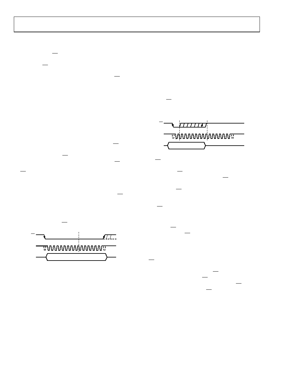
NORMAL MODE
This mode is intended for fastest throughput rate performance.
The user does not have to worry about any power-up times with
the AD7452 remaining fully powered up all the time. Figure 36
shows the general diagram of the AD7452’s operation in this
mode. The conversion is initiated on the falling edge of CS, as
described in the Serial Interface section. To ensure that the part
remains fully powered up, CS must remain low until at least 10
SCLK falling edges have elapsed after the falling edge of CS.
If CS is brought high any time after the 10th SCLK falling edge,
but before the 16th SCLK falling edge, the part remains powered
up but the conversion is terminated and SDATA goes back into
three-state. Sixteen serial clock cycles are required to complete
the conversion and access the complete conversion result. CS
may idle high until the next conversion or may idle low until
sometime prior to the next conversion. Once a data transfer is
complete, i.e., when SDATA has returned to three-state, another
conversion can be initiated after the quiet time, tQUIET, has
elapsed by again bringing CS low.
110
CS
SCLK
SDATA
16
4 LEADING ZEROS + CONVERSION RESULT
03154-A
-036
Figure 36. Normal Mode Operation
POWER-DOWN MODE
This mode is intended for use in applications where slower
throughput rates are required; either the ADC is powered down
between each conversion, or a series of conversions may be
performed at a high throughput rate and the ADC is then
powered down for a relatively long duration between these
bursts of several conversions. When the AD7452 is in power-
down mode, all analog circuitry is powered down. To enter
power-down mode, the conversion process must be interrupted
by bringing CS high anywhere after the second falling edge of
SCLK, and before the 10th falling edge of SCLK, as shown in
1
10
CS
SCLK
SDATA
THREE-STATE
2
03154-A
-037
Figure 37. Entering Power-Down Mode
Once CS has been brought high in this window of SCLKs, the
part enters power-down, the conversion that was initiated by
the falling edge of CS is terminated, and SDATA goes back into
three-state. The time from the rising edge of CS to SDATA
Specifications). If CS is brought high before the second SCLK
falling edge, the part remains in normal mode and does not
power down. This avoids accidental power-down due to glitches
on the CS line.
In order to exit this mode of operation and power up the
AD7452 again, a dummy conversion is performed. On the
falling edge of CS, the device begins to power up and continues
to power up as long as CS is held low until after the falling edge
of the 10th SCLK. The device is fully powered up after 1 s has
elapsed and, as shown in Figure 38, valid data results from the
next conversion.
If CS is brought high before the 10th falling edge of SCLK, the
AD7452 again goes back into power-down. This avoids acci-
dental power-up due to glitches on the CS line or an inadvertent
burst of eight SCLK cycles while CS is low. So although the
device may begin to power up on the falling edge of CS, it again
powers down on the rising edge of CS as long as it occurs before
the 10th SCLK falling edge.
相关PDF资料 |
PDF描述 |
|---|---|
| PX0921/04/S | CONN RCPT 4POS W/SOCKET |
| VE-JT4-MW-F3 | CONVERTER MOD DC/DC 48V 100W |
| SP3245ECY-L | IC TXRX RS233 28TSSOP |
| VE-JVY-MY-F4 | CONVERTER MOD DC/DC 3.3V 33W |
| VE-JT4-MW-F1 | CONVERTER MOD DC/DC 48V 100W |
相关代理商/技术参数 |
参数描述 |
|---|---|
| AD7452BRTZ-REEL7 | 功能描述:IC ADC 12BIT DIF 555KSPS SOT23-8 RoHS:是 类别:集成电路 (IC) >> 数据采集 - 模数转换器 系列:- 标准包装:2,500 系列:- 位数:16 采样率(每秒):15 数据接口:MICROWIRE?,串行,SPI? 转换器数目:1 功率耗散(最大):480µW 电压电源:单电源 工作温度:-40°C ~ 85°C 安装类型:表面贴装 封装/外壳:38-WFQFN 裸露焊盘 供应商设备封装:38-QFN(5x7) 包装:带卷 (TR) 输入数目和类型:16 个单端,双极;8 个差分,双极 配用:DC1011A-C-ND - BOARD DELTA SIGMA ADC LTC2494 |
| AD7453 | 制造商:AD 制造商全称:Analog Devices 功能描述:Pseudo Differential, 555 kSPS, 12-Bit ADC in an 8-Lead SOT-23 |
| AD7453ART-REEL7 | 制造商:Analog Devices 功能描述: |
| AD7453ARTZ-REEL7 | 功能描述:IC ADC 12BIT DFF 600KSPS SOT23-8 RoHS:是 类别:集成电路 (IC) >> 数据采集 - 模数转换器 系列:- 标准包装:2,500 系列:- 位数:16 采样率(每秒):15 数据接口:MICROWIRE?,串行,SPI? 转换器数目:1 功率耗散(最大):480µW 电压电源:单电源 工作温度:-40°C ~ 85°C 安装类型:表面贴装 封装/外壳:38-WFQFN 裸露焊盘 供应商设备封装:38-QFN(5x7) 包装:带卷 (TR) 输入数目和类型:16 个单端,双极;8 个差分,双极 配用:DC1011A-C-ND - BOARD DELTA SIGMA ADC LTC2494 |
| AD7453BRT-R2 | 制造商:Analog Devices 功能描述:ADC Single SAR 555ksps 12-bit Serial 8-Pin SOT-23 T/R 制造商:Rochester Electronics LLC 功能描述:12-BIT P/DIFF I/PUT, 600KSPS ADC I.C. - Bulk |
发布紧急采购,3分钟左右您将得到回复。