- 您现在的位置:买卖IC网 > PDF目录10222 > AD7472BRUZ (Analog Devices Inc)IC ADC 12BIT PARALLEL 24TSSOP PDF资料下载
参数资料
| 型号: | AD7472BRUZ |
| 厂商: | Analog Devices Inc |
| 文件页数: | 11/21页 |
| 文件大小: | 0K |
| 描述: | IC ADC 12BIT PARALLEL 24TSSOP |
| 标准包装: | 62 |
| 位数: | 12 |
| 采样率(每秒): | 1.5M |
| 数据接口: | 并联 |
| 转换器数目: | 1 |
| 功率耗散(最大): | 12mW |
| 电压电源: | 模拟和数字 |
| 工作温度: | -40°C ~ 85°C |
| 安装类型: | 表面贴装 |
| 封装/外壳: | 24-TSSOP(0.173",4.40mm 宽) |
| 供应商设备封装: | 24-TSSOP |
| 包装: | 管件 |
| 输入数目和类型: | 1 个单端,单极 |
REV. B
AD7470/AD7472
–18–
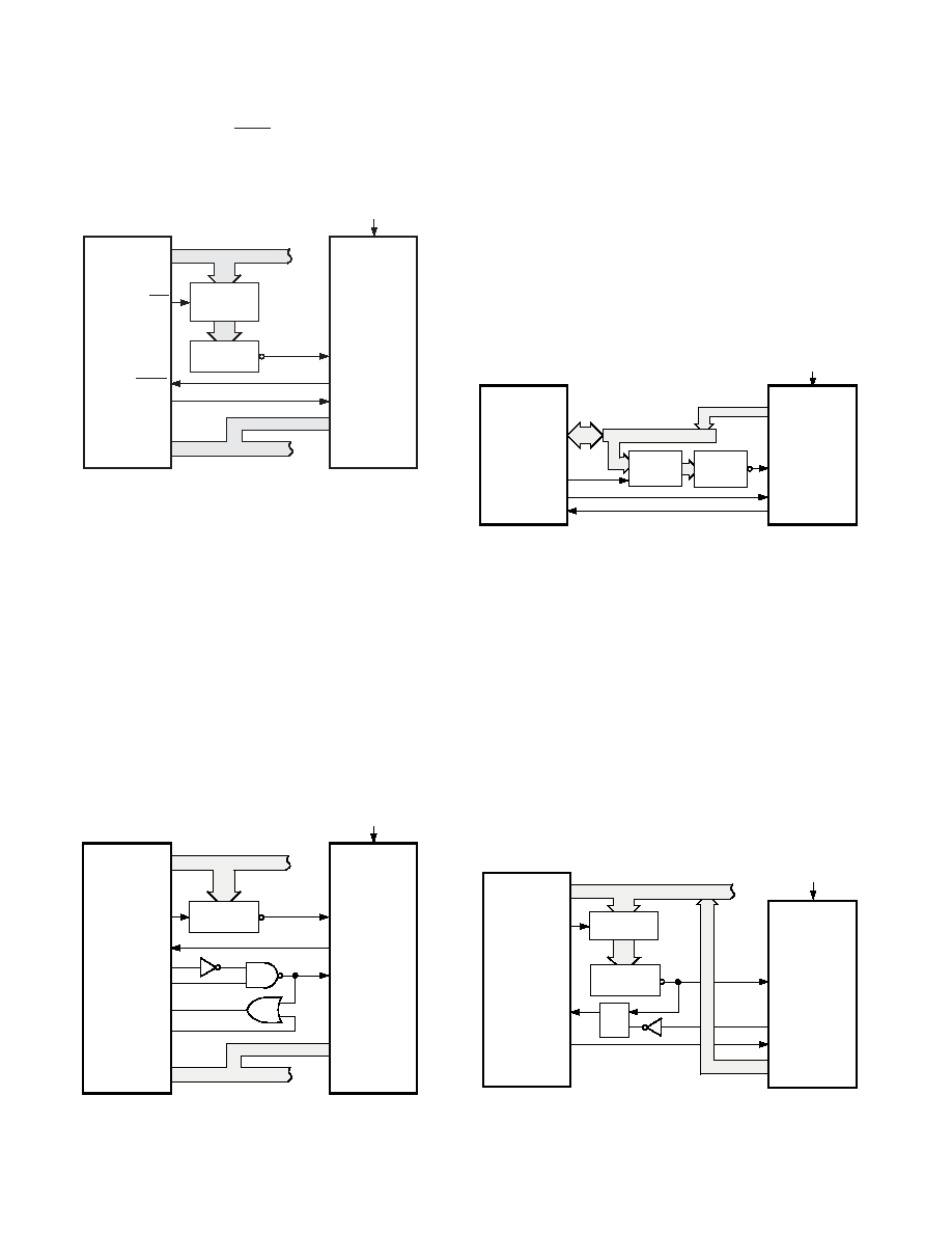
control line is actually three memory select lines. Internal
ADDR25–24 are decoded into MS3-0; these lines are then asserted
as chip selects. The
DMAR
1 (DMA Request 1) is used in this
setup as the interrupt to signal end of conversion. The rest of
the interface is standard handshaking operation.
AD7470/
AD7472*
ADSP-21065L*
ADDR0–ADDR23
RD
D0–D31
CONVST
RD
BUSY
DB0–DB9
(DB11)
ADDRESS BUS
DATA BUS
*ADDITIONAL PINS OMITTED FOR CLARITY
OPTIONAL
DMAR1
ADDRESS
LATCH
ADDRESS
BUS
ADDRESS
DECODER
MSX
CS
Figure 18. Interfacing to ADSP-21065L
AD7470/AD7472 to TMS320C25 Interface
Figure 19 shows an interface between the AD7470/AD7472
and the TMS320C25. The
CONVST signal can be applied
from the TMS320C25 or from an external source. The BUSY
line interrupts the digital signal processor when conversion is
completed. The TMS320C25 does not have a separate
RD
output to drive the AD7470/AD7472
RD input directly. This
has to be generated from the processor
STRB and R/W outputs
with the addition of some glue logic. The
RD signal is OR-gated
with the
MSC signal to provide the WAIT state required in the
read cycle for correct interface timing. The following instruction
is used to read the conversion from the AD7470/AD7472:
IN D,ADC
where D is data memory address and ADC is the AD7470/
AD7472 address. The read operation must not be attempted
during conversion.
ADDRESS
DECODER
AD7470/
AD7472*
TMS320C25*
A0–A15
IS
STRB
R/
W
READY
DMD0–DMD15
CONVST
CS
RD
BUSY
DB0–DB9
(DB11)
ADDRESS BUS
*ADDITIONAL PINS OMITTED FOR CLARITY
OPTIONAL
MSC
DATA BUS
Figure 19. Interfacing to the TMS320C25
AD7470/AD7472 to PIC17C4x Interface
Figure 20 shows a typical parallel interface between the AD7470/
AD7472 and the PIC17C42/43/44. The microcontroller sees
the ADC as another memory device with its own specific
memory address on the memory map. The
CONVST signal can
be controlled by either the microcontroller or an external
source. The BUSY signal provides an interrupt request to the
microcontroller when a conversion ends. The INT pin on the
PIC17C42/43/44 must be configured to be active on the nega-
tive edge. PORTC and PORTD of the microcontroller are
bidirectional and used to address the AD7470/AD7472 and also
to read in the 10-bit (AD7470) or 12-bit (AD7472) data. The
OE pin on the PIC can be used to enable the output buffers on
the AD7470/AD7472 and to perform a read operation.
*ADDITIONAL PINS OMITTED FOR CLARITY
ADDRESS
DECODER
ADDRESS
LATCH
OPTIONAL
PIC17C4x*
AD0–AD15
OE
INT
AD7470/
AD7472*
CONVST
CS
RD
BUSY
DB0–DB9
(DB11)
ALE
Figure 20. Interfacing to the PIC17C4x
AD7470/AD7472 to 80C186 Interface
Figure 21 shows the AD7470/AD7472 interfaced to the 80C186
microprocessor. The 80C186 DMA controller provides two
independent high speed DMA channels where data transfer
can occur between memory and I/O spaces. (The AD7470/
AD7472 occupies one of these I/O spaces.) Each data trans-
fer consumes two bus cycles, one cycle to fetch data and the
other to store data.
After the AD7470/AD7472 has finished conversion, the BUSY
line generates a DMA request to Channel 1 (DRQ1). As a result
of the interrupt, the processor performs a DMA READ opera-
tion which also resets the interrupt latch. Sufficient priority
must be assigned to the DMA channel to ensure that the DMA
request will be serviced before the completion of the next con-
version. This configuration can be used with 6 MHz and 8 MHz
80C186 processors.
80C186*
AD0–AD15
A16–A19
RD
DRQ1
ADDRESS/DATA BUS
DATA BUS
*ADDITIONAL PINS OMITTED FOR CLARITY
ADDRESS
LATCH
ADDRESS
BUS
ADDRESS
DECODER
ALE
R
S
Q
AD7470/
AD7472*
CONVST
RD
BUSY
DB0–DB9
(DB11)
OPTIONAL
CS
Figure 21. Interfacing to the 80C186
相关PDF资料 |
PDF描述 |
|---|---|
| GTC06A-16S-1P | CONN PLUG 7POS STRAIGHT W/PINS |
| VI-B13-MY | CONVERTER MOD DC/DC 24V 50W |
| VE-2NM-CU-F1 | CONVERTER MOD DC/DC 10V 200W |
| 14282-20PG-300 | CONN RCPT 20POS PNL MNT PIN |
| SP3243EBEY-L/TR | IC TXRX RS232 INTELLIGNT 28TSSOP |
相关代理商/技术参数 |
参数描述 |
|---|---|
| AD7472BRUZ-REEL | 功能描述:IC ADC 12BIT PARALLEL 24TSSOP RoHS:是 类别:集成电路 (IC) >> 数据采集 - 模数转换器 系列:- 标准包装:1,000 系列:- 位数:16 采样率(每秒):45k 数据接口:串行 转换器数目:2 功率耗散(最大):315mW 电压电源:模拟和数字 工作温度:0°C ~ 70°C 安装类型:表面贴装 封装/外壳:28-SOIC(0.295",7.50mm 宽) 供应商设备封装:28-SOIC W 包装:带卷 (TR) 输入数目和类型:2 个单端,单极 |
| AD7472BRUZ-REEL7 | 功能描述:IC ADC 12BIT PARALLEL 24TSSOP RoHS:是 类别:集成电路 (IC) >> 数据采集 - 模数转换器 系列:- 标准包装:1,000 系列:- 位数:16 采样率(每秒):45k 数据接口:串行 转换器数目:2 功率耗散(最大):315mW 电压电源:模拟和数字 工作温度:0°C ~ 70°C 安装类型:表面贴装 封装/外壳:28-SOIC(0.295",7.50mm 宽) 供应商设备封装:28-SOIC W 包装:带卷 (TR) 输入数目和类型:2 个单端,单极 |
| AD7472BRZ | 功能描述:IC ADC 12BIT PARALLEL 24SOIC RoHS:是 类别:集成电路 (IC) >> 数据采集 - 模数转换器 系列:- 标准包装:1,000 系列:- 位数:12 采样率(每秒):300k 数据接口:并联 转换器数目:1 功率耗散(最大):75mW 电压电源:单电源 工作温度:0°C ~ 70°C 安装类型:表面贴装 封装/外壳:24-SOIC(0.295",7.50mm 宽) 供应商设备封装:24-SOIC 包装:带卷 (TR) 输入数目和类型:1 个单端,单极;1 个单端,双极 |
| AD7472YR | 制造商:Analog Devices 功能描述:ADC Single SAR 1.5Msps 12-bit Parallel 24-Pin SOIC W 制造商:Rochester Electronics LLC 功能描述:12 BIT 1.5MSPS PARALLEL ADC I.C. - Bulk |
| AD7472YR-REEL | 功能描述:IC ADC 12BIT PARALLEL 24-SOIC RoHS:否 类别:集成电路 (IC) >> 数据采集 - 模数转换器 系列:- 标准包装:1,000 系列:- 位数:12 采样率(每秒):300k 数据接口:并联 转换器数目:1 功率耗散(最大):75mW 电压电源:单电源 工作温度:0°C ~ 70°C 安装类型:表面贴装 封装/外壳:24-SOIC(0.295",7.50mm 宽) 供应商设备封装:24-SOIC 包装:带卷 (TR) 输入数目和类型:1 个单端,单极;1 个单端,双极 |
发布紧急采购,3分钟左右您将得到回复。