- 您现在的位置:买卖IC网 > PDF目录10222 > AD7472BRUZ (Analog Devices Inc)IC ADC 12BIT PARALLEL 24TSSOP PDF资料下载
参数资料
| 型号: | AD7472BRUZ |
| 厂商: | Analog Devices Inc |
| 文件页数: | 6/21页 |
| 文件大小: | 0K |
| 描述: | IC ADC 12BIT PARALLEL 24TSSOP |
| 标准包装: | 62 |
| 位数: | 12 |
| 采样率(每秒): | 1.5M |
| 数据接口: | 并联 |
| 转换器数目: | 1 |
| 功率耗散(最大): | 12mW |
| 电压电源: | 模拟和数字 |
| 工作温度: | -40°C ~ 85°C |
| 安装类型: | 表面贴装 |
| 封装/外壳: | 24-TSSOP(0.173",4.40mm 宽) |
| 供应商设备封装: | 24-TSSOP |
| 包装: | 管件 |
| 输入数目和类型: | 1 个单端,单极 |
REV. B
AD7470/AD7472
–13–
OPERATING MODES
The AD7470 and AD7472 have two possible modes of opera-
tion, depending on the state of the
CONVST pulse at the end of
a conversion, Mode 1 and Mode 2. There is a continuous clock
on the CLKIN pin.
Mode 1 (High Speed Sampling)
In this mode of operation, the
CONVST pulse is brought high
before the end of conversion i.e., before BUSY goes low (see
Figure 10). If the
CONVST pin is brought from high to low
while BUSY is high, the conversion is restarted. When operat-
ing in this mode, a new conversion should not be initiated until
the acquisition time has elapsed after BUSY goes low. This
acquisition time allows the track-and-hold circuit to accurately
acquire the input signal. As mentioned earlier, a read should
not be done during a conversion. This mode facilitates the
fastest throughput times for the AD7470/AD7472.
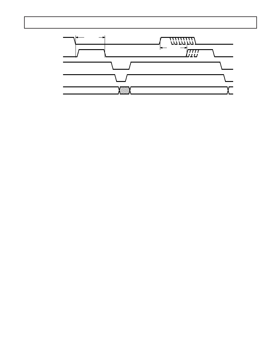
Mode 2 (Sleep Mode)
Figure 13 shows AD7470/AD7472 in Mode 2 operation where
the ADC goes into sleep mode after conversion. The
CONVST
line is brought low to initiate a conversion and remains low until
after the end of conversion. If
CONVST goes high and low
again while BUSY is high, the conversion is restarted. Once the
BUSY line goes from a high to a low, the
CONVST line has its
status checked and, if low, the part enters sleep mode.
The device wakes up again on the rising edge of the
CONVST
signal. There is a wake-up time of typically 1
s after the rising
edge of
CONVST before the BUSY line can go high to indicate
start of conversion. BUSY will only go high once
CONVST goes
low. The
CONVST line can go from a high to a low during this
wake-up time, but the conversion will still not be initiated until
after the 1
s wake-up time. Superior power performance can be
achieved in this mode of operation by waking up the AD7470
and AD7472 only to carry out a conversion.
Burst Mode
Burst mode on the AD7470/AD7472 is a subsection of Mode 1
and Mode 2; the clock is noncontinuous. Figure 12 shows how
the ADC works in burst mode for Mode 2. The clock needs to
be switched on only during conversion, a minimum of 12 clock
cycles for the AD7470 and 14 clock cycles for the AD7472.
Because the clock is off during nonconverting intervals, system
power is saved. The BUSY signal can be used to gate the CLKIN
pulses. The ADC does not begin the conversion process until
CONVST
BUSY
CS
RD
DBx
tWAKEUP
tCONVERT
Figure 13. Mode 2 Operation
the first CLKIN rising edge after BUSY goes high. The clock
needs to start less than two clock cycles away from the
CONVST active edge, otherwise INL deteriorates. For
example, if the clock frequency is 28 MHz, the clock must start
within 71.4 ns of
CONVST going low. In Figure 12, the A/D
converter section is put into sleep mode once conversion is
completed. On the rising edge of
CONVST, it is woken up
again. The user must be wary of the wake-up time because it
will reduce the sampling rate of the ADC.
VDRIVE
The VDRIVE pin is used as the voltage supply to the output driv-
ers and is a separate supply from AVDD and DVDD. The purpose
of using a separate supply for the output drivers is that the user
can vary the output high voltage, VOH, from the VDD supply to
the AD7470/AD7472. For example, if AVDD and DVDD is using
a 5 V supply, the VDRIVE pin can be powered from a 3 V supply.
The ADC has better dynamic performance at 5 V than at 3 V,
so operating the part at 5 V, while still being able to interface to
3 V parts, pushes the AD7470/AD7472 to the top bracket of
high performance 10-bit/12-bit ADCs. Of course, the ADC can
have its VDRIVE and DVDD pins connected together and be pow-
ered from a 3 V or 5 V supply.
All outputs are powered from VDRIVE. These are all the data out
pins and the BUSY pin. The
CONVST, CS, RD, and CLKIN
signals are related to the DVDD voltage.
POWER-UP
It is recommended that the user perform a dummy conversion
after power-up, because the first conversion result could be
incorrect. This also ensures that the part is in the correct mode
of operation. The recommended power-up sequence is as
follows:
1. GND
4. Digital Inputs
2. VDD
5. REF IN
3. VDRIVE
6. VIN
Power vs. Throughput
The two modes of operation for the AD7470 and AD7472 will
produce different power versus throughput performances,
Mode 1 and Mode 2; see Operating Modes section of the data
sheet for more detailed descriptions of these modes. Mode 2 is
the sleep mode of the part and it achieves the optimum power
performance.
相关PDF资料 |
PDF描述 |
|---|---|
| GTC06A-16S-1P | CONN PLUG 7POS STRAIGHT W/PINS |
| VI-B13-MY | CONVERTER MOD DC/DC 24V 50W |
| VE-2NM-CU-F1 | CONVERTER MOD DC/DC 10V 200W |
| 14282-20PG-300 | CONN RCPT 20POS PNL MNT PIN |
| SP3243EBEY-L/TR | IC TXRX RS232 INTELLIGNT 28TSSOP |
相关代理商/技术参数 |
参数描述 |
|---|---|
| AD7472BRUZ-REEL | 功能描述:IC ADC 12BIT PARALLEL 24TSSOP RoHS:是 类别:集成电路 (IC) >> 数据采集 - 模数转换器 系列:- 标准包装:1,000 系列:- 位数:16 采样率(每秒):45k 数据接口:串行 转换器数目:2 功率耗散(最大):315mW 电压电源:模拟和数字 工作温度:0°C ~ 70°C 安装类型:表面贴装 封装/外壳:28-SOIC(0.295",7.50mm 宽) 供应商设备封装:28-SOIC W 包装:带卷 (TR) 输入数目和类型:2 个单端,单极 |
| AD7472BRUZ-REEL7 | 功能描述:IC ADC 12BIT PARALLEL 24TSSOP RoHS:是 类别:集成电路 (IC) >> 数据采集 - 模数转换器 系列:- 标准包装:1,000 系列:- 位数:16 采样率(每秒):45k 数据接口:串行 转换器数目:2 功率耗散(最大):315mW 电压电源:模拟和数字 工作温度:0°C ~ 70°C 安装类型:表面贴装 封装/外壳:28-SOIC(0.295",7.50mm 宽) 供应商设备封装:28-SOIC W 包装:带卷 (TR) 输入数目和类型:2 个单端,单极 |
| AD7472BRZ | 功能描述:IC ADC 12BIT PARALLEL 24SOIC RoHS:是 类别:集成电路 (IC) >> 数据采集 - 模数转换器 系列:- 标准包装:1,000 系列:- 位数:12 采样率(每秒):300k 数据接口:并联 转换器数目:1 功率耗散(最大):75mW 电压电源:单电源 工作温度:0°C ~ 70°C 安装类型:表面贴装 封装/外壳:24-SOIC(0.295",7.50mm 宽) 供应商设备封装:24-SOIC 包装:带卷 (TR) 输入数目和类型:1 个单端,单极;1 个单端,双极 |
| AD7472YR | 制造商:Analog Devices 功能描述:ADC Single SAR 1.5Msps 12-bit Parallel 24-Pin SOIC W 制造商:Rochester Electronics LLC 功能描述:12 BIT 1.5MSPS PARALLEL ADC I.C. - Bulk |
| AD7472YR-REEL | 功能描述:IC ADC 12BIT PARALLEL 24-SOIC RoHS:否 类别:集成电路 (IC) >> 数据采集 - 模数转换器 系列:- 标准包装:1,000 系列:- 位数:12 采样率(每秒):300k 数据接口:并联 转换器数目:1 功率耗散(最大):75mW 电压电源:单电源 工作温度:0°C ~ 70°C 安装类型:表面贴装 封装/外壳:24-SOIC(0.295",7.50mm 宽) 供应商设备封装:24-SOIC 包装:带卷 (TR) 输入数目和类型:1 个单端,单极;1 个单端,双极 |
发布紧急采购,3分钟左右您将得到回复。