参数资料
| 型号: | AD7564BN |
| 厂商: | Analog Devices Inc |
| 文件页数: | 15/17页 |
| 文件大小: | 0K |
| 描述: | IC DAC 12BIT QUAD 5V LP 28-DIP |
| 产品培训模块: | Data Converter Fundamentals DAC Architectures |
| 标准包装: | 13 |
| 设置时间: | 500ns |
| 位数: | 12 |
| 数据接口: | 串行 |
| 转换器数目: | 4 |
| 电压电源: | 单电源 |
| 功率耗散(最大): | 50µW |
| 工作温度: | -40°C ~ 85°C |
| 安装类型: | 通孔 |
| 封装/外壳: | 28-DIP(0.600",15.24mm) |
| 供应商设备封装: | 28-PDIP |
| 包装: | 管件 |
| 输出数目和类型: | 8 电流,单极;8 电流,双极 |
| 采样率(每秒): | 1.8M |
AD7564
REV. B
–7–
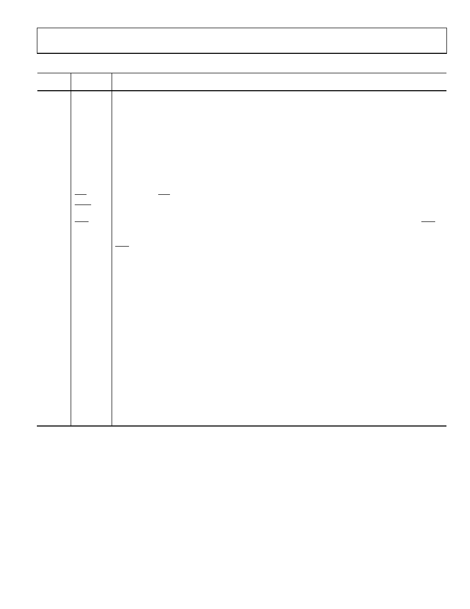
PIN DESCRIPTIONS
Pin
Number
Mnemonic
Description
1
DGND
Digital Ground.
2
IOUT2C
IOUT2 terminal for DAC C. This should normally connect to the signal ground of the system.
3
VDD
Positive power supply. This is +5 V ± 5%.
4
IOUT1C
IOUT1 terminal for DAC C.
5
RFBC
Feedback resistor for DAC C.
6
VREFC
DAC C reference input.
7
IOUT2D
IOUT2 terminal for DAC D. This should normally connect to the signal ground of the system.
8
IOUT1D
IOUT1 terminal for DAC D.
9
RFBD
Feedback resistor for DAC D.
10
VREFD
DAC D reference input.
11
SDOUT
This shift register output allows multiple devices to be connected in a daisy chain configuration.
12
CLR
Asynchronous CLR input. When this input is taken low, all DAC latches are loaded with all 0s.
13
LDAC
Asynchronous LDAC input. When this input is taken low, all DAC latches are simultaneously updated with the
contents of the input latches.
14
FSIN
Level-triggered control input (active low). This is the frame synchronization signal for the input data. When FSIN
goes low, it enables the input shift register, and data is transferred on the falling edges of CLKIN. If the address
bits are valid, the 12-bit DAC data is transferred to the appropriate input latch on the sixteenth falling edge after
FSIN goes low.
15
SDIN
Serial data input. The device accepts a 16-bit word. DB0 and DB1 are DAC select bits. DB2 and DB3 are device
address bits. DB4 to DB15 contain the 12-bit data to be loaded to the selected DAC.
16
CLKIN
Clock Input. Data is clocked into the input shift register on the falling edges of CLKIN. Add a pull-down resistor on
the clock line to avoid timing issues.
17
A1
Device address pin. This input in association with A0 gives the device an address. If DB2 and DB3 of the serial
input stream do not correspond to this address, the data which follows is ignored and not loaded to any input
latch. However, it will appear at SDOUT irrespective of this.
18
A0
Device address pin. This input in association with A1 gives the device an address.
19
VREFA
DAC A reference input.
20
RFBA
Feedback resistor for DAC A.
21
IOUT1A
IOUT1 terminal for DAC A.
22
IOUT2A
IOUT2 terminal for DAC A. This should normally connect to the signal ground of the system.
23
VREFB
DAC B reference input.
24
RFBB
Feedback resistor for DAC B.
25
IOUT1B
IOUT1 terminal for DAC B.
26
N/C
No Connect pin.
27
AGND
This pin connects to the back gates of the current steering switches. It should be connected to the signal ground
of the system.
28
IOUT2B
IOUT2 terminal for DAC B. This should normally connect to the signal ground of the system.
相关PDF资料 |
PDF描述 |
|---|---|
| AD7569JRZ-REEL | IC I/O PORT 8BIT ANALOG 24SOIC |
| AD7581KN | IC DAS 8BIT 8CH 5V 28-DIP |
| AD7606BSTZ | IC DAS W/ADC 16BIT 8CH 64LQFP |
| AD7607BSTZ-RL | IC DAS W/ADC 14BIT 8CH 64LQFP |
| AD7608BSTZ-RL | IC DAS W/ADC 18BIT 8CH 64LQFP |
相关代理商/技术参数 |
参数描述 |
|---|---|
| AD7564BNZ | 功能描述:IC DAC 12BIT QUAD 5V LP 28DIP RoHS:是 类别:集成电路 (IC) >> 数据采集 - 数模转换器 系列:- 标准包装:1 系列:- 设置时间:4.5µs 位数:12 数据接口:串行,SPI? 转换器数目:1 电压电源:单电源 功率耗散(最大):- 工作温度:-40°C ~ 125°C 安装类型:表面贴装 封装/外壳:8-SOIC(0.154",3.90mm 宽) 供应商设备封装:8-SOICN 包装:剪切带 (CT) 输出数目和类型:1 电压,单极;1 电压,双极 采样率(每秒):* 其它名称:MCP4921T-E/SNCTMCP4921T-E/SNRCTMCP4921T-E/SNRCT-ND |
| AD7564BR | 功能描述:IC DAC 12BIT LC2MOS QUAD 28-SOIC RoHS:否 类别:集成电路 (IC) >> 数据采集 - 数模转换器 系列:- 产品培训模块:Data Converter Fundamentals DAC Architectures 标准包装:750 系列:- 设置时间:7µs 位数:16 数据接口:并联 转换器数目:1 电压电源:双 ± 功率耗散(最大):100mW 工作温度:0°C ~ 70°C 安装类型:表面贴装 封装/外壳:28-LCC(J 形引线) 供应商设备封装:28-PLCC(11.51x11.51) 包装:带卷 (TR) 输出数目和类型:1 电压,单极;1 电压,双极 采样率(每秒):143k |
| AD7564BR-REEL | 功能描述:IC DAC 12BIT QUAD 5V LP 28-SOIC RoHS:否 类别:集成电路 (IC) >> 数据采集 - 数模转换器 系列:- 产品培训模块:Data Converter Fundamentals DAC Architectures 标准包装:750 系列:- 设置时间:7µs 位数:16 数据接口:并联 转换器数目:1 电压电源:双 ± 功率耗散(最大):100mW 工作温度:0°C ~ 70°C 安装类型:表面贴装 封装/外壳:28-LCC(J 形引线) 供应商设备封装:28-PLCC(11.51x11.51) 包装:带卷 (TR) 输出数目和类型:1 电压,单极;1 电压,双极 采样率(每秒):143k |
| AD7564BRS | 功能描述:IC DAC 12BIT LC2MOS QUAD 28-SSOP RoHS:否 类别:集成电路 (IC) >> 数据采集 - 数模转换器 系列:- 产品培训模块:Data Converter Fundamentals DAC Architectures 标准包装:750 系列:- 设置时间:7µs 位数:16 数据接口:并联 转换器数目:1 电压电源:双 ± 功率耗散(最大):100mW 工作温度:0°C ~ 70°C 安装类型:表面贴装 封装/外壳:28-LCC(J 形引线) 供应商设备封装:28-PLCC(11.51x11.51) 包装:带卷 (TR) 输出数目和类型:1 电压,单极;1 电压,双极 采样率(每秒):143k |
| AD7564BRS-REEL | 功能描述:IC DAC 12BIT QUAD 5V LP 28-SSOP RoHS:否 类别:集成电路 (IC) >> 数据采集 - 数模转换器 系列:- 产品培训模块:Data Converter Fundamentals DAC Architectures 标准包装:750 系列:- 设置时间:7µs 位数:16 数据接口:并联 转换器数目:1 电压电源:双 ± 功率耗散(最大):100mW 工作温度:0°C ~ 70°C 安装类型:表面贴装 封装/外壳:28-LCC(J 形引线) 供应商设备封装:28-PLCC(11.51x11.51) 包装:带卷 (TR) 输出数目和类型:1 电压,单极;1 电压,双极 采样率(每秒):143k |
发布紧急采购,3分钟左右您将得到回复。