参数资料
| 型号: | AD7564BN |
| 厂商: | Analog Devices Inc |
| 文件页数: | 3/17页 |
| 文件大小: | 0K |
| 描述: | IC DAC 12BIT QUAD 5V LP 28-DIP |
| 产品培训模块: | Data Converter Fundamentals DAC Architectures |
| 标准包装: | 13 |
| 设置时间: | 500ns |
| 位数: | 12 |
| 数据接口: | 串行 |
| 转换器数目: | 4 |
| 电压电源: | 单电源 |
| 功率耗散(最大): | 50µW |
| 工作温度: | -40°C ~ 85°C |
| 安装类型: | 通孔 |
| 封装/外壳: | 28-DIP(0.600",15.24mm) |
| 供应商设备封装: | 28-PDIP |
| 包装: | 管件 |
| 输出数目和类型: | 8 电流,单极;8 电流,双极 |
| 采样率(每秒): | 1.8M |
–11–
REV.
3
AD7564
GENERAL DESCRIPTION
D/A Section
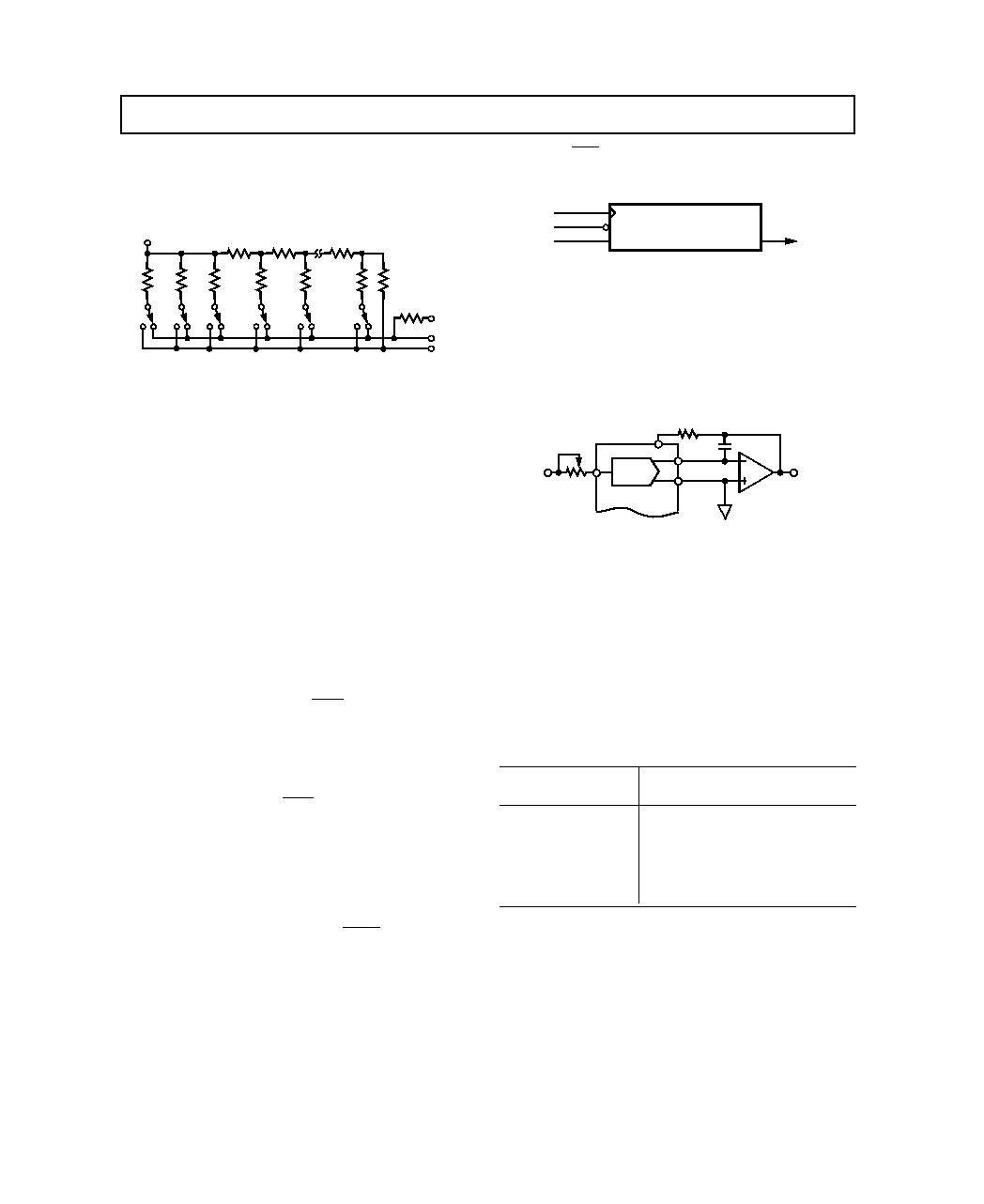
The AD7564 contains four 12-bit current output D/A convert-
ers. A simplified circuit diagram for one of the D/A converters
is shown in Figure 15.
VREF
2R
CB
A
S9
S8
S0
RFB
I OUT1
I OUT2
R
R/2
SHOWN FOR ALL 1s ON DAC
Figure 15. Simplified D/A Circuit Diagram
A segmented scheme is used whereby the 2 MSBs of the 12-bit
data word are decoded to drive the three switches A, B and C.
The remaining 10 bits of the data word drive the switches S0 to
S9 in a standard R-2R ladder configuration.
Each of the switches A to C steers 1/4 of the total reference
current with the remaining current passing through the R-2R
section.
All DACs have separate VREF, IOUT1, IOUT2 and RFB pins.
When an output amplifier is connected in the standard configu-
ration of Figure 17, the output voltage is given by:
VOUT = D ×VREF
where D is the fractional representation of the digital word
loaded to the DAC. Thus, in the AD7564, D can be set from 0
to 4095/4096.
Interface Section
The AD7564 is a serial input device. Three input signals con-
trol the serial interface. These are FSIN, CLKIN and SDIN.
The timing diagram is shown in Figure 1.
Data applied to the SDIN pin is clocked into the input shift reg-
ister on each falling edge of CLKIN. SDOUT is the shift regis-
ter output. It allows multiple devices to be connected in a daisy
chain fashion with the SDOUT pin of one device connected to
the SDIN of the next device. FSIN is the frame synchronization
for the device.
When the sixteen bits have been received in the input shift regis-
ter, DB2 and DB3 (A0 and A1) are checked to see if they corre-
spond to the state on pins A0 and A1. If it does, then the word
is accepted. Otherwise, it is disregarded. This allows the user
to address a number of AD7564s in a very simple fashion. DB1
and DB0 of the 16-bit word determine which of the four DAC
input latches is to be loaded. When the LDAC line goes low, all
four DAC latches in the device are simultaneously loaded with
the contents of their respective input latches and the outputs
change accordingly.
Bringing the CLR line low resets the DAC latches to all 0s. The
input latches are not affected so that the user can revert to the
previous analog output if desired.
16-BIT INPUT
SHIFT REGISTER
CLKIN
FSIN
SDIN
SDOUT
Figure 16. Input Logic
UNIPOLAR BINARY OPERATION
(2-Quadrant Multiplication)
Figure 17 shows the standard unipolar binary connection dia-
gram for one of the DACs in the AD7564. When VIN is an ac
signal, the circuit performs 2-quadrant multiplication. Resistors
R1 and R2 allow the user to adjust the DAC gain error. Offset
can be removed by adjusting the output amplifier offset voltage.
Figure 17. Unipolar Binary Operation
A1 should be chosen to suit the application. For example, the
AD707 is ideal for very low bandwidth applications while the
AD843 and AD845 offer very fast settling time in wide band-
width applications. Appropriate multiple versions of these am-
plifiers can be used with the AD7564 to reduce board space
requirements.
The code table for Figure 17 is shown in Table III.
Table III. Unipolar Binary Code Table
Digital Input
Analog Output
MSB . . . LSB
(VOUT as Shown in Figure 17)
1111 1111 1111
–VREF (4095/4096)
1000 0000 0001
–VREF (2049/4096)
1000 0000 0000
–VREF (2048/4096)
0111 1111 1111
–VREF (2047/4096)
0000 0000 0001
–VREF (1/4096)
0000 0000 0000
–VREF (0/4096) = 0
NOTE
Nominal LSB size for the circuit of Figure 17 is given by: VREF (1/4096).
DAC A
A1
AD7564
VREFA
VIN
NOTES
1. ONLY ONE DAC IS SHOWN FOR CLARITY.
2. DIGITAL INPUT CONNECTIONS ARE OMITTED.
3. C1 PHASE COMPENSATION (5–15pF) MAY BE
REQUIRED WHEN USING HIGH SPEED AMPLIFIER.
R2 10
R1 20
SIGNAL
GND
A1: AD707
AD711
AD843
AD845
C1
RFBA
IOUT2A
IOUT1A
VOUT
B
相关PDF资料 |
PDF描述 |
|---|---|
| AD7569JRZ-REEL | IC I/O PORT 8BIT ANALOG 24SOIC |
| AD7581KN | IC DAS 8BIT 8CH 5V 28-DIP |
| AD7606BSTZ | IC DAS W/ADC 16BIT 8CH 64LQFP |
| AD7607BSTZ-RL | IC DAS W/ADC 14BIT 8CH 64LQFP |
| AD7608BSTZ-RL | IC DAS W/ADC 18BIT 8CH 64LQFP |
相关代理商/技术参数 |
参数描述 |
|---|---|
| AD7564BNZ | 功能描述:IC DAC 12BIT QUAD 5V LP 28DIP RoHS:是 类别:集成电路 (IC) >> 数据采集 - 数模转换器 系列:- 标准包装:1 系列:- 设置时间:4.5µs 位数:12 数据接口:串行,SPI? 转换器数目:1 电压电源:单电源 功率耗散(最大):- 工作温度:-40°C ~ 125°C 安装类型:表面贴装 封装/外壳:8-SOIC(0.154",3.90mm 宽) 供应商设备封装:8-SOICN 包装:剪切带 (CT) 输出数目和类型:1 电压,单极;1 电压,双极 采样率(每秒):* 其它名称:MCP4921T-E/SNCTMCP4921T-E/SNRCTMCP4921T-E/SNRCT-ND |
| AD7564BR | 功能描述:IC DAC 12BIT LC2MOS QUAD 28-SOIC RoHS:否 类别:集成电路 (IC) >> 数据采集 - 数模转换器 系列:- 产品培训模块:Data Converter Fundamentals DAC Architectures 标准包装:750 系列:- 设置时间:7µs 位数:16 数据接口:并联 转换器数目:1 电压电源:双 ± 功率耗散(最大):100mW 工作温度:0°C ~ 70°C 安装类型:表面贴装 封装/外壳:28-LCC(J 形引线) 供应商设备封装:28-PLCC(11.51x11.51) 包装:带卷 (TR) 输出数目和类型:1 电压,单极;1 电压,双极 采样率(每秒):143k |
| AD7564BR-REEL | 功能描述:IC DAC 12BIT QUAD 5V LP 28-SOIC RoHS:否 类别:集成电路 (IC) >> 数据采集 - 数模转换器 系列:- 产品培训模块:Data Converter Fundamentals DAC Architectures 标准包装:750 系列:- 设置时间:7µs 位数:16 数据接口:并联 转换器数目:1 电压电源:双 ± 功率耗散(最大):100mW 工作温度:0°C ~ 70°C 安装类型:表面贴装 封装/外壳:28-LCC(J 形引线) 供应商设备封装:28-PLCC(11.51x11.51) 包装:带卷 (TR) 输出数目和类型:1 电压,单极;1 电压,双极 采样率(每秒):143k |
| AD7564BRS | 功能描述:IC DAC 12BIT LC2MOS QUAD 28-SSOP RoHS:否 类别:集成电路 (IC) >> 数据采集 - 数模转换器 系列:- 产品培训模块:Data Converter Fundamentals DAC Architectures 标准包装:750 系列:- 设置时间:7µs 位数:16 数据接口:并联 转换器数目:1 电压电源:双 ± 功率耗散(最大):100mW 工作温度:0°C ~ 70°C 安装类型:表面贴装 封装/外壳:28-LCC(J 形引线) 供应商设备封装:28-PLCC(11.51x11.51) 包装:带卷 (TR) 输出数目和类型:1 电压,单极;1 电压,双极 采样率(每秒):143k |
| AD7564BRS-REEL | 功能描述:IC DAC 12BIT QUAD 5V LP 28-SSOP RoHS:否 类别:集成电路 (IC) >> 数据采集 - 数模转换器 系列:- 产品培训模块:Data Converter Fundamentals DAC Architectures 标准包装:750 系列:- 设置时间:7µs 位数:16 数据接口:并联 转换器数目:1 电压电源:双 ± 功率耗散(最大):100mW 工作温度:0°C ~ 70°C 安装类型:表面贴装 封装/外壳:28-LCC(J 形引线) 供应商设备封装:28-PLCC(11.51x11.51) 包装:带卷 (TR) 输出数目和类型:1 电压,单极;1 电压,双极 采样率(每秒):143k |
发布紧急采购,3分钟左右您将得到回复。