- 您现在的位置:买卖IC网 > PDF目录10089 > AD7612BCPZ-RL (Analog Devices Inc)IC ADC 16BIT 750KSPS SAR 48LFCSP PDF资料下载
参数资料
| 型号: | AD7612BCPZ-RL |
| 厂商: | Analog Devices Inc |
| 文件页数: | 20/32页 |
| 文件大小: | 0K |
| 描述: | IC ADC 16BIT 750KSPS SAR 48LFCSP |
| 标准包装: | 2,500 |
| 系列: | PulSAR® |
| 位数: | 16 |
| 采样率(每秒): | 750k |
| 数据接口: | 串行,并联 |
| 转换器数目: | 1 |
| 功率耗散(最大): | 230mW |
| 电压电源: | 模拟和数字 |
| 工作温度: | -40°C ~ 85°C |
| 安装类型: | 表面贴装 |
| 封装/外壳: | 48-VFQFN 裸露焊盘,CSP |
| 供应商设备封装: | 48-LFCSP-VQ(7x7) |
| 包装: | 带卷 (TR) |
| 输入数目和类型: | 1 个差分,双极 |
| 配用: | EVAL-AD7612CBZ-ND - BOARD EVALUATION FOR AD7612 |
第1页第2页第3页第4页第5页第6页第7页第8页第9页第10页第11页第12页第13页第14页第15页第16页第17页第18页第19页当前第20页第21页第22页第23页第24页第25页第26页第27页第28页第29页第30页第31页第32页
Data Sheet
AD7612
Rev. A | Page 27 of 32
SLAVE SERIAL INTERFACE
The pins multiplexed on D[11:4] used for slave serial
interface are: EXT/INT, INVSCLK, SDIN, SDOUT,
SDCLK and RDERROR.
External Clock (SER/PAR = High, EXT/INT = High)
Setting the EXT/INT = high allows the AD7612 to accept an
externally supplied serial data clock on the SDCLK pin. In this
mode, several methods can be used to read the data. The exter-
nal serial clock is gated by CS. When CS and RD are both low,
the data can be read after each conversion or during the following
conversion. A clock can be either normally high or normally low
when inactive. For detailed timing diagrams, see Figure 42 and
While the AD7612 is performing a bit decision, it is important
that voltage transients be avoided on digital input/output pins,
or degradation of the conversion result may occur. This is par-
ticularly important during the last 475 ns of the conversion phase
because the AD7612 provides error correction circuitry that can
correct for an improper bit decision made during the first part
of the conversion phase. For this reason, it is recommended that
any external clock provided, is a discontinuous clock that transi-
tions only when BUSY is low, or, more importantly, that it does not
transition during the last 475 ns of BUSY high.
External Discontinuous Clock Data Read After
Conversion
Though the maximum throughput cannot be achieved using
this mode, it is the most recommended of the serial slave modes.
Figure 42 shows the detailed timing diagrams for this method.
After a conversion is complete, indicated by BUSY returning low,
the conversion result can be read while both CS and RD are low.
Data is shifted out MSB first with 16 clock pulses and, depending
on the SDCLK frequency, can be valid on the falling and rising
edges of the clock.
One advantage of this method is that conversion performance is
not degraded because there are no voltage transients on the digital
interface during the conversion process. Another advantage is
the ability to read the data at any speed up to 40 MHz, which
accommodates both the slow digital host interface and the fastest
serial reading.
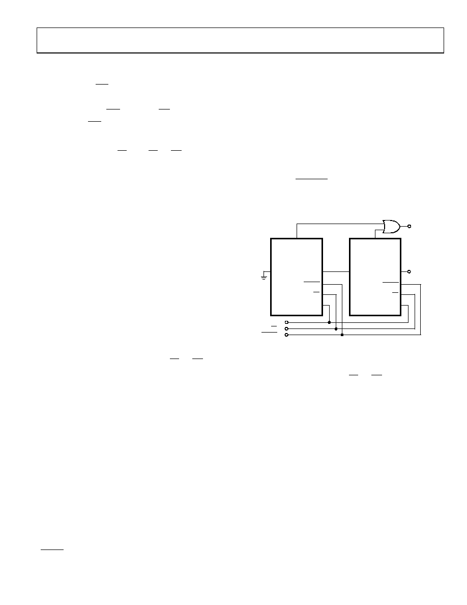
Daisy-Chain Feature
Also in the read after convert mode, the AD7612 provides a daisy-
chain feature for cascading multiple converters together using
the serial data input, SDIN, pin. This feature is useful for reduce-
ing component count and wiring connections when desired, for
instance, in isolated multiconverter applications. See Figure 42
for the timing details.
An example of the concatenation of two devices is shown in
Figure 41. Simultaneous sampling is possible by using a common
CNVST signal. Note that the SDIN input is latched on the opposite
edge of SDCLK used to shift out the data on SDOUT (SDCLK
falling edge when INVSCLK = low). Therefore, the MSB of the
upstream converter follows the LSB of the downstream con-
verter on the next SDCLK cycle. In this mode, the 40 MHz
SDCLK rate cannot be used since the SDIN to SDCLK setup
time, t33, is less than the minimum time specified. (SDCLK to
SDOUT delay, t32, is the same for all converters when simul-
taneously sampled). For proper operation, the SDCLK edge for
latching SDIN (or period of SDCLK) needs to be:
33
32
SDCLK
t
2
/
1
Or the max SDCLK frequency needs to be:
)
(
2
1
33
32
SDCLK
t
f
If not using the daisy-chain feature, the SDIN input should be
tied either high or low.
SCLK
SDOUT
RDC/SDIN
AD7612
#1
(DOWNSTREAM)
AD7612
#2
(UPSTREAM)
BUSY
OUT
BUSY
DATA
OUT
SCLK
RDC/SDIN
SDOUT
SCLK IN
CNVST IN
CNVST
CS
CNVST
CS
CS IN
0
62
65
-04
1
Figure 41. Two AD7612 Devices in a Daisy-Chain Configuration
External Clock Data Read During Previous Conversion
Figure 43 shows the detailed timing diagrams for this method.
During a conversion, while both CS and RD are low, the result
of the previous conversion can be read. Data is shifted out MSB
first with 16 clock pulses and, depending on the SDCLK frequency,
can be valid on the falling and rising edges of the clock. The
16 bits have to be read before the current conversion is complete;
otherwise, RDERROR is pulsed high and can be used to interrupt
the host interface to prevent incomplete data reading.
To reduce performance degradation due to digital activity, a fast
discontinuous clock of at least 40 MHz is recommended to ensure
that all the bits are read during the first half of the SAR
conversion phase.
The daisy-chain feature should not be used in this mode since
digital activity occurs during the second half of the SAR
conversion phase likely resulting in performance degradation.
相关PDF资料 |
PDF描述 |
|---|---|
| MS27467E17A35PB | CONN PLUG 55POS STRAIGHT W/PINS |
| LTC1480IS8#TR | IC TXRX RS485 3.3V ULT LP 8SOIC |
| VE-B62-MW-F2 | CONVERTER MOD DC/DC 15V 100W |
| VI-2TZ-MY | CONVERTER MOD DC/DC 2V 20W |
| IDT72241L15PF8 | IC FIFO 2048X18 SYNC 15NS 32QFP |
相关代理商/技术参数 |
参数描述 |
|---|---|
| AD7612BST | 制造商:Analog Devices 功能描述:ADC 16BIT 750KSPS SAR 48-LQFP 制造商:Analog Devices 功能描述:ADC, 16BIT, 750KSPS, SAR, 48-LQFP |
| AD7612BSTZ | 功能描述:IC ADC 16BIT 750KSPS SAR 48-LQFP RoHS:是 类别:集成电路 (IC) >> 数据采集 - 模数转换器 系列:PulSAR® 其它有关文件:TSA1204 View All Specifications 标准包装:1 系列:- 位数:12 采样率(每秒):20M 数据接口:并联 转换器数目:2 功率耗散(最大):155mW 电压电源:模拟和数字 工作温度:-40°C ~ 85°C 安装类型:表面贴装 封装/外壳:48-TQFP 供应商设备封装:48-TQFP(7x7) 包装:Digi-Reel® 输入数目和类型:4 个单端,单极;2 个差分,单极 产品目录页面:1156 (CN2011-ZH PDF) 其它名称:497-5435-6 |
| AD7612BSTZ-RL | 功能描述:IC ADC 16BIT 750KSPS SAR 48-LQFP RoHS:是 类别:集成电路 (IC) >> 数据采集 - 模数转换器 系列:PulSAR® 标准包装:1 系列:- 位数:14 采样率(每秒):83k 数据接口:串行,并联 转换器数目:1 功率耗散(最大):95mW 电压电源:双 ± 工作温度:0°C ~ 70°C 安装类型:通孔 封装/外壳:28-DIP(0.600",15.24mm) 供应商设备封装:28-PDIP 包装:管件 输入数目和类型:1 个单端,双极 |
| AD7616BSTZ | 功能描述:16 Bit Analog to Digital Converter 16 Input 2 SAR 80-LQFP (14x14) 制造商:analog devices inc. 系列:- 包装:托盘 零件状态:在售 位数:16 采样率(每秒):1M 输入数:16 输入类型:差分 数据接口:SPI,并联,DSP 配置:MUX-S/H-ADC 无线电 - S/H:ADC:1:1 A/D 转换器数:2 架构:SAR 参考类型:外部, 内部 电压 - 电源,模拟:5V 电压 - 电源,数字:2.3 V ~ 3.6 V 特性:同步采样 工作温度:-40°C ~ 125°C 封装/外壳:80-LQFP 供应商器件封装:80-LQFP(14x14) 标准包装:1 |
| AD7616BSTZ-RL | 功能描述:16 Bit Analog to Digital Converter 16 Input 2 SAR 80-LQFP (14x14) 制造商:analog devices inc. 系列:- 包装:剪切带(CT) 零件状态:在售 位数:16 采样率(每秒):1M 输入数:16 输入类型:差分 数据接口:SPI,并联,DSP 配置:MUX-S/H-ADC 无线电 - S/H:ADC:1:1 A/D 转换器数:2 架构:SAR 参考类型:外部, 内部 电压 - 电源,模拟:5V 电压 - 电源,数字:2.3 V ~ 3.6 V 特性:同步采样 工作温度:-40°C ~ 125°C 封装/外壳:80-LQFP 供应商器件封装:80-LQFP(14x14) 标准包装:1 |
发布紧急采购,3分钟左右您将得到回复。