- 您现在的位置:买卖IC网 > PDF目录10089 > AD7612BCPZ-RL (Analog Devices Inc)IC ADC 16BIT 750KSPS SAR 48LFCSP PDF资料下载
参数资料
| 型号: | AD7612BCPZ-RL |
| 厂商: | Analog Devices Inc |
| 文件页数: | 9/32页 |
| 文件大小: | 0K |
| 描述: | IC ADC 16BIT 750KSPS SAR 48LFCSP |
| 标准包装: | 2,500 |
| 系列: | PulSAR® |
| 位数: | 16 |
| 采样率(每秒): | 750k |
| 数据接口: | 串行,并联 |
| 转换器数目: | 1 |
| 功率耗散(最大): | 230mW |
| 电压电源: | 模拟和数字 |
| 工作温度: | -40°C ~ 85°C |
| 安装类型: | 表面贴装 |
| 封装/外壳: | 48-VFQFN 裸露焊盘,CSP |
| 供应商设备封装: | 48-LFCSP-VQ(7x7) |
| 包装: | 带卷 (TR) |
| 输入数目和类型: | 1 个差分,双极 |
| 配用: | EVAL-AD7612CBZ-ND - BOARD EVALUATION FOR AD7612 |
第1页第2页第3页第4页第5页第6页第7页第8页当前第9页第10页第11页第12页第13页第14页第15页第16页第17页第18页第19页第20页第21页第22页第23页第24页第25页第26页第27页第28页第29页第30页第31页第32页
Data Sheet
AD7612
Rev. A | Page 17 of 32
THEORY OF OPERATION
SWA
SWB
IN+
REF
REFGND
LSB
MSB
32,768C
IN–
16,384C
4C
2C
C
65,536C
CONTROL
LOGIC
SWITCHES
CONTROL
BUSY
OUTPUT
CODE
CNVST
COMP
06
26
5-
02
5
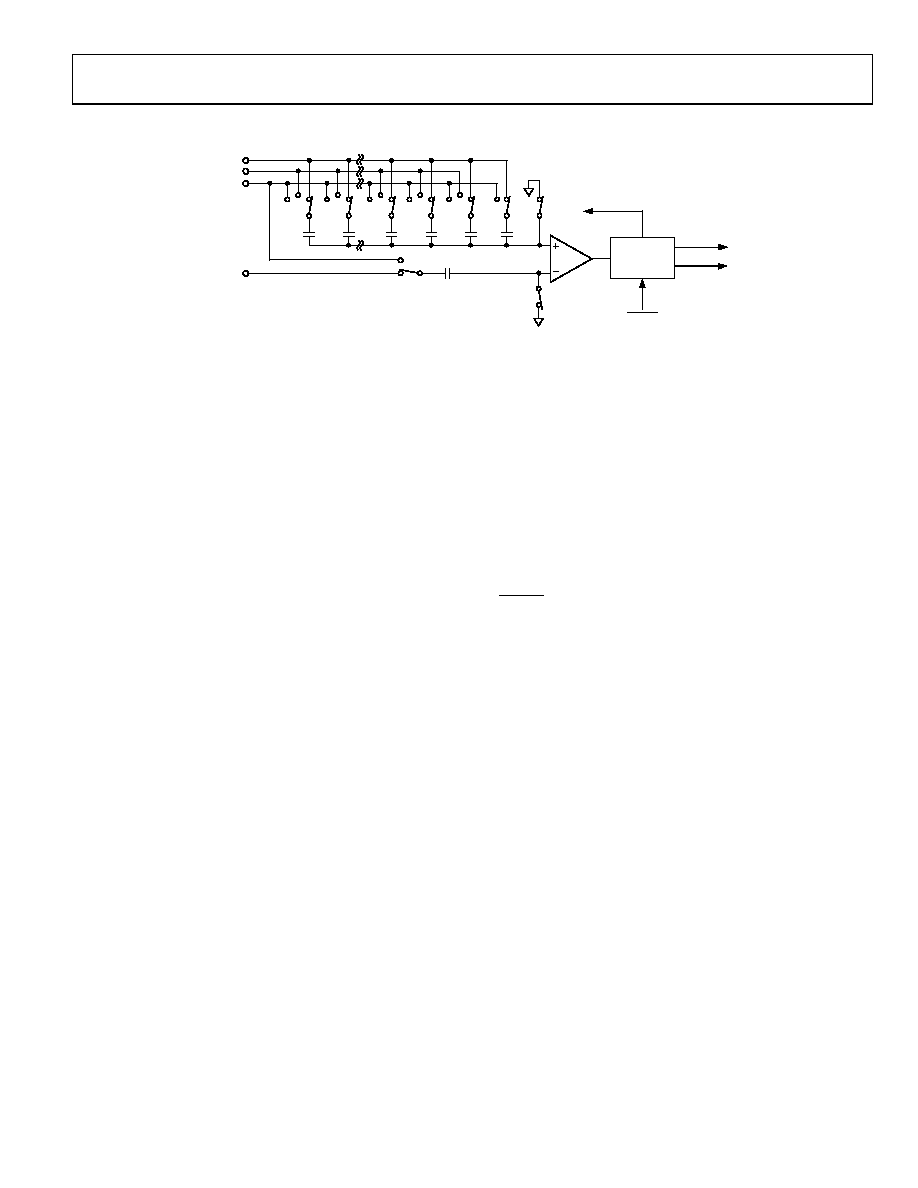
Figure 25. ADC Simplified Schematic
OVERVIEW
The AD7612 is a very fast, low power, precise, 16-bit analog-to-
digital converter (ADC) using successive approximation capacitive
digital-to-analog (CDAC) architecture.
The AD7612 can be configured at any time for one of four input
ranges and conversion mode with inputs in parallel and serial
hardware modes or by a dedicated write only, SPI-compatible
interface via a configuration register in serial software mode.
The AD7612 uses Analog Device’s patented iCMOS high voltage
process to accommodate 0 to 5 V, 0 to 10 V, ±5 V, and ±10 V
input ranges without the use of conventional thin films. Only
one acquisition cycle, t8, is required for the inputs to latch to the
correct configuration. Resetting or power cycling is not
required for reconfiguring the ADC.
The AD7612 features different modes to optimize performance
according to the applications. It is capable of converting 750,000
samples per second (750 kSPS) in warp mode, 600 kSPS in normal
mode, and 500 kSPS in impulse mode.
The AD7612 provides the user with an on-chip track-and-hold,
successive approximation ADC that does not exhibit any pipe-
line or latency, making it ideal for multiple multiplexed channel
applications.
For unipolar input ranges, the AD7612 typically requires three
supplies; VCC, AVDD (which can supply DVDD), and OVDD
which can be interfaced to either 5 V, 3.3 V, or 2.5 V digital logic.
For bipolar input ranges, the AD7612 requires the use of the
additional VEE supply.
The device is housed in Pb-free, 48-lead LQFP or tiny LFCSP
7 mm × 7 mm packages that combine space savings with flexi-
bility. In addition, the AD7612 can be configured as either a
parallel or serial SPI-compatible interface.
CONVERTER OPERATION
The AD7612 is a successive approximation ADC based on a
charge redistribution DAC. Figure 25 shows the simplified
schematic of the ADC. The CDAC consists of two identical
arrays of 16 binary weighted capacitors, which are connected
to the two comparator inputs.
During the acquisition phase, terminals of the array tied to the
comparator’s input are connected to AGND via SW+ and SW.
All independent switches are connected to the analog inputs.
Thus, the capacitor arrays are used as sampling capacitors and
acquire the analog signal on IN+ and IN inputs. A conversion
phase is initiated once the acquisition phase is complete and the
CNVST input goes low. When the conversion phase begins, SW+
and SW are opened first. The two capacitor arrays are then
disconnected from the inputs and connected to the REFGND
input. Therefore, the differential voltage between the inputs
(IN+ and IN) captured at the end of the acquisition phase is
applied to the comparator inputs, causing the comparator to
become unbalanced. By switching each element of the capacitor
array between REFGND and REF, the comparator input varies
by binary weighted voltage steps (VREF/2, VREF/4 through VREF/
65536). The control logic toggles these switches, starting with
the MSB first, in order to bring the comparator back into a
balanced condition.
After the completion of this process, the control logic generates
the ADC output code and brings the BUSY output low.
相关PDF资料 |
PDF描述 |
|---|---|
| MS27467E17A35PB | CONN PLUG 55POS STRAIGHT W/PINS |
| LTC1480IS8#TR | IC TXRX RS485 3.3V ULT LP 8SOIC |
| VE-B62-MW-F2 | CONVERTER MOD DC/DC 15V 100W |
| VI-2TZ-MY | CONVERTER MOD DC/DC 2V 20W |
| IDT72241L15PF8 | IC FIFO 2048X18 SYNC 15NS 32QFP |
相关代理商/技术参数 |
参数描述 |
|---|---|
| AD7612BST | 制造商:Analog Devices 功能描述:ADC 16BIT 750KSPS SAR 48-LQFP 制造商:Analog Devices 功能描述:ADC, 16BIT, 750KSPS, SAR, 48-LQFP |
| AD7612BSTZ | 功能描述:IC ADC 16BIT 750KSPS SAR 48-LQFP RoHS:是 类别:集成电路 (IC) >> 数据采集 - 模数转换器 系列:PulSAR® 其它有关文件:TSA1204 View All Specifications 标准包装:1 系列:- 位数:12 采样率(每秒):20M 数据接口:并联 转换器数目:2 功率耗散(最大):155mW 电压电源:模拟和数字 工作温度:-40°C ~ 85°C 安装类型:表面贴装 封装/外壳:48-TQFP 供应商设备封装:48-TQFP(7x7) 包装:Digi-Reel® 输入数目和类型:4 个单端,单极;2 个差分,单极 产品目录页面:1156 (CN2011-ZH PDF) 其它名称:497-5435-6 |
| AD7612BSTZ-RL | 功能描述:IC ADC 16BIT 750KSPS SAR 48-LQFP RoHS:是 类别:集成电路 (IC) >> 数据采集 - 模数转换器 系列:PulSAR® 标准包装:1 系列:- 位数:14 采样率(每秒):83k 数据接口:串行,并联 转换器数目:1 功率耗散(最大):95mW 电压电源:双 ± 工作温度:0°C ~ 70°C 安装类型:通孔 封装/外壳:28-DIP(0.600",15.24mm) 供应商设备封装:28-PDIP 包装:管件 输入数目和类型:1 个单端,双极 |
| AD7616BSTZ | 功能描述:16 Bit Analog to Digital Converter 16 Input 2 SAR 80-LQFP (14x14) 制造商:analog devices inc. 系列:- 包装:托盘 零件状态:在售 位数:16 采样率(每秒):1M 输入数:16 输入类型:差分 数据接口:SPI,并联,DSP 配置:MUX-S/H-ADC 无线电 - S/H:ADC:1:1 A/D 转换器数:2 架构:SAR 参考类型:外部, 内部 电压 - 电源,模拟:5V 电压 - 电源,数字:2.3 V ~ 3.6 V 特性:同步采样 工作温度:-40°C ~ 125°C 封装/外壳:80-LQFP 供应商器件封装:80-LQFP(14x14) 标准包装:1 |
| AD7616BSTZ-RL | 功能描述:16 Bit Analog to Digital Converter 16 Input 2 SAR 80-LQFP (14x14) 制造商:analog devices inc. 系列:- 包装:剪切带(CT) 零件状态:在售 位数:16 采样率(每秒):1M 输入数:16 输入类型:差分 数据接口:SPI,并联,DSP 配置:MUX-S/H-ADC 无线电 - S/H:ADC:1:1 A/D 转换器数:2 架构:SAR 参考类型:外部, 内部 电压 - 电源,模拟:5V 电压 - 电源,数字:2.3 V ~ 3.6 V 特性:同步采样 工作温度:-40°C ~ 125°C 封装/外壳:80-LQFP 供应商器件封装:80-LQFP(14x14) 标准包装:1 |
发布紧急采购,3分钟左右您将得到回复。