参数资料
| 型号: | AD7631BCPZ |
| 厂商: | Analog Devices Inc |
| 文件页数: | 19/32页 |
| 文件大小: | 0K |
| 描述: | IC ADC 18BIT 250KSPS BIP 48LFCSP |
| 标准包装: | 1 |
| 系列: | PulSAR® |
| 位数: | 18 |
| 采样率(每秒): | 250k |
| 数据接口: | 串行,并联 |
| 转换器数目: | 1 |
| 功率耗散(最大): | 120mW |
| 电压电源: | 模拟和数字 |
| 工作温度: | -40°C ~ 85°C |
| 安装类型: | 表面贴装 |
| 封装/外壳: | 48-VFQFN 裸露焊盘,CSP |
| 供应商设备封装: | 48-LFCSP-VQ(7x7) |
| 包装: | 托盘 |
| 输入数目和类型: | 1 个差分,单极;1 个差分,双极 |
第1页第2页第3页第4页第5页第6页第7页第8页第9页第10页第11页第12页第13页第14页第15页第16页第17页第18页当前第19页第20页第21页第22页第23页第24页第25页第26页第27页第28页第29页第30页第31页第32页
AD7631
Data Sheet
Rev. B | Page 26 of 32
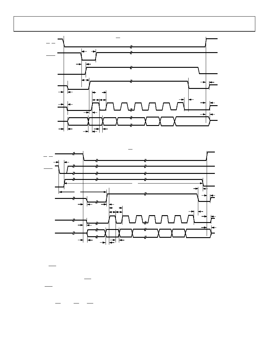
EXT/INT = 0
RDC/SDIN = 1
INVSCLK = INVSYNC = 0
D17
D16
D2
D1
D0
X
12
3
16
17
18
BUSY
SYNC
SDCLK
SDOUT
CNVST
CS, RD
t23
t18
t15
t14
t17
t3
t22
t16
t1
t25
t26
t24
t27
t19
t20 t21
MODE[1:0] = 3
06
58
8-
04
1
Figure 41. Master Serial Data Timing for Reading (Read Previous Conversion During Convert)
BUSY
SYNC
SDCLK
SDOUT
12
3
16
17
18
D17
D16
D2
D1
D0
X
RDC/SDIN = 0
INVSCLK = INVSYNC = 0
CNVST
CS, RD
EXT/INT = 0
t23
t22
t16
t15
t14
t29
t19
t21
t20
t18
t28
t30
t24
t25
t26
t27
t3
MODE[1:0] = 3
06
58
8-
04
2
Figure 42. Master Serial Data Timing for Reading (Read After Convert)
SLAVE SERIAL INTERFACE
The pins multiplexed on D[13:6] used for slave serial
interface are: EXT/INT, INVSCLK, SDIN, SDOUT, SDCLK,
and RDERROR.
External Clock (MODE[1:0] = 3, EXT/INT = High)
Setting the EXT/INT = high allows the AD7631 to accept an
externally supplied serial data clock on the SDCLK pin. In this
mode, several methods can be used to read the data. The external
serial clock is gated by CS. When CS and RD are both low, the
data can be read after each conversion or during the following
conversion. A clock can be either normally high or normally
low when inactive. For detailed timing diagrams, see Figure 44
and Figure 45.
While the AD7631 is performing a bit decision, it is important
that voltage transients be avoided on digital input/output pins,
or degradation of the conversion result may occur. This is
particularly important during the last 550 ns of the conversion
phase because the AD7631 provides error correction circuitry
that can correct for an improper bit decision made during
the first part of the conversion phase. For this reason, it is
recommended that any external clock provided is a
discontinuous clock that transitions only when BUSY is low,
or, more importantly, that it does not transition during the
last 450 ns of BUSY high.
相关PDF资料 |
PDF描述 |
|---|---|
| AD7634BCPZ | IC ADC 18BIT BIPO PROGR 48-LFCSP |
| AD7641BSTZRL | IC ADC 18BIT 2MSPS SAR 48-LQFP |
| AD7643BCPZ | IC ADC 18BIT DIFF W/REF 48LFCSP |
| AD7650ACPZ | IC ADC 16BIT CMOS 5V 48LFCSP |
| AD7651ACPZ | IC ADC 16BIT UNIPOLAR 48LFCSP |
相关代理商/技术参数 |
参数描述 |
|---|---|
| AD7631BCPZRL | 功能描述:IC ADC 18BIT 250KSPS BIP 48LFCSP RoHS:是 类别:集成电路 (IC) >> 数据采集 - 模数转换器 系列:PulSAR® 标准包装:1 系列:- 位数:14 采样率(每秒):83k 数据接口:串行,并联 转换器数目:1 功率耗散(最大):95mW 电压电源:双 ± 工作温度:0°C ~ 70°C 安装类型:通孔 封装/外壳:28-DIP(0.600",15.24mm) 供应商设备封装:28-PDIP 包装:管件 输入数目和类型:1 个单端,双极 |
| AD7631BSTZ | 功能描述:IC ADC 18BIT 250KSPS BIP 48-LQFP RoHS:是 类别:集成电路 (IC) >> 数据采集 - 模数转换器 系列:PulSAR® 其它有关文件:TSA1204 View All Specifications 标准包装:1 系列:- 位数:12 采样率(每秒):20M 数据接口:并联 转换器数目:2 功率耗散(最大):155mW 电压电源:模拟和数字 工作温度:-40°C ~ 85°C 安装类型:表面贴装 封装/外壳:48-TQFP 供应商设备封装:48-TQFP(7x7) 包装:Digi-Reel® 输入数目和类型:4 个单端,单极;2 个差分,单极 产品目录页面:1156 (CN2011-ZH PDF) 其它名称:497-5435-6 |
| AD7631BSTZRL | 功能描述:IC ADC 18BIT 250KSPS BIP 48-LQFP RoHS:是 类别:集成电路 (IC) >> 数据采集 - 模数转换器 系列:PulSAR® 标准包装:1 系列:- 位数:14 采样率(每秒):83k 数据接口:串行,并联 转换器数目:1 功率耗散(最大):95mW 电压电源:双 ± 工作温度:0°C ~ 70°C 安装类型:通孔 封装/外壳:28-DIP(0.600",15.24mm) 供应商设备封装:28-PDIP 包装:管件 输入数目和类型:1 个单端,双极 |
| AD7634 | 制造商:AD 制造商全称:Analog Devices 功能描述:14-Bit, 1 MSPS, Differential, Programmable Input PulSAR ADC |
| AD7634BCPZ | 功能描述:IC ADC 18BIT BIPO PROGR 48-LFCSP RoHS:是 类别:集成电路 (IC) >> 数据采集 - 模数转换器 系列:PulSAR® 标准包装:1 系列:- 位数:14 采样率(每秒):83k 数据接口:串行,并联 转换器数目:1 功率耗散(最大):95mW 电压电源:双 ± 工作温度:0°C ~ 70°C 安装类型:通孔 封装/外壳:28-DIP(0.600",15.24mm) 供应商设备封装:28-PDIP 包装:管件 输入数目和类型:1 个单端,双极 |
发布紧急采购,3分钟左右您将得到回复。