- 您现在的位置:买卖IC网 > PDF目录10667 > AD7658BSTZ (Analog Devices Inc)IC ADC 12BIT 6CH 250KSPS 64LQFP PDF资料下载
参数资料
| 型号: | AD7658BSTZ |
| 厂商: | Analog Devices Inc |
| 文件页数: | 13/32页 |
| 文件大小: | 0K |
| 描述: | IC ADC 12BIT 6CH 250KSPS 64LQFP |
| 标准包装: | 1 |
| 位数: | 12 |
| 采样率(每秒): | 250k |
| 数据接口: | 串行,并联 |
| 转换器数目: | 6 |
| 功率耗散(最大): | 143mW |
| 电压电源: | 模拟和数字,双 ± |
| 工作温度: | -40°C ~ 85°C |
| 安装类型: | 表面贴装 |
| 封装/外壳: | 64-LQFP |
| 供应商设备封装: | 64-LQFP(10x10) |
| 包装: | 托盘 |
| 输入数目和类型: | 6 个单端,双极 |
| 产品目录页面: | 778 (CN2011-ZH PDF) |
| 配用: | EVAL-AD7658CBZ-ND - BOARD EVAL FOR AD7658 |
第1页第2页第3页第4页第5页第6页第7页第8页第9页第10页第11页第12页当前第13页第14页第15页第16页第17页第18页第19页第20页第21页第22页第23页第24页第25页第26页第27页第28页第29页第30页第31页第32页
AD7656/AD7657/AD7658
Data Sheet
Rev. D | Page 20 of 32
THEORY OF OPERATION
CONVERTER DETAILS
The AD7656/AD7657/AD7658 are high speed, low power
converters that allow the simultaneous sampling of six on-chip
ADCs. The analog inputs on the AD7656/AD7657/AD7658 can
accept true bipolar input signals. The RANGE pin/RNG bits are
used to select either ±4 × VREF or ±2 × VREF as the input range
for the next conversion.
Each AD7656/AD7657/AD7658 contains six SAR ADCs, six
track-and-hold amplifiers, an on-chip 2.5 V reference, reference
buffers, and high speed parallel and serial interfaces. The parts
allow the simultaneous sampling of all six ADCs when all three
CONVST signals are tied together. Alternatively, the six ADCs
can be grouped into three pairs. Each pair has an associated
CONVST signal used to initiate simultaneous sampling on each
ADC pair, on four ADCs, or on all six ADCs. CONVST A is used
to initiate simultaneous sampling on V1 and V2, CONVST B
is used to initiate simultaneous sampling on V3 and V4, and
CONVST C is used to initiate simultaneous sampling on V5
and V6.
A conversion is initiated on the AD7656/AD7657/AD7658 by
pulsing the CONVST x input. On the rising edge of CONVST x,
the track-and-hold of the selected ADC pair is placed into hold
mode and the conversions are started. After the rising edge of
CONVST x, the BUSY signal goes high to indicate that the
conversion is taking place. The conversion clock for the
AD7656/AD7657/AD7658 is internally generated, and the
conversion time for the parts is 3 s. The BUSY signal returns
low to indicate the end of conversion. On the falling edge of
BUSY, the track-and-hold returns to track mode. Data can be
read from the output register via the parallel or serial interface.
Track-and-Hold Section
The track-and-hold amplifiers on the AD7656/AD7657/AD7658
allow the ADCs to accurately convert an input sine wave of full-
scale amplitude to 16-/14-/12-bit resolution, respectively. The
input bandwidth of the track-and-hold amplifiers is greater
than the Nyquist rate of the ADC, even when the AD7656/
AD7657/AD7658 are operating at its maximum throughput
rate. The parts can handle input frequencies of up to 12 MHz.
The track-and-hold amplifiers sample their respective inputs
simultaneously on the rising edge of CONVSTx. The aperture time
for the track-and-hold (that is, the delay time between the external
CONVSTx signal actually going into hold) is 10 ns. This is well
matched across all six track-and-holds on one device and from
device to device. This allows more than six ADCs to be sampled
simultaneously. The end of the conversion is signaled by the falling
edge of BUSY, and it is at this point that the track-and-holds return
to track mode and the acquisition time begins.
Analog Input Section
The AD7656/AD7657/AD7658 can handle true bipolar input
voltages. The logic level on the RANGE pin or the value written
to the RNGx bits in the control register determines the analog
input range on the AD7656/AD7657/AD7658 for the next
conversion. When the RANGE pin/RNGx bit is 1, the analog
input range for the next conversion is ±2 × VREF. When the
RANGE pin/RNGx bit is 0, the analog input range for the next
conversion is ±4 × VREF.
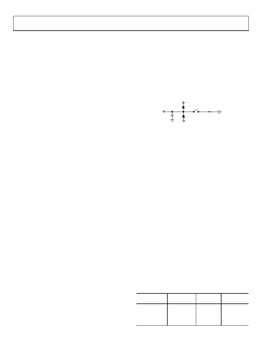
D1
D2
VDD
C2
R1
V1
VSS
C1
05020-
004
Figure 24. Equivalent Analog Input Structure
Figure 24 shows an equivalent circuit of the analog input structure
of the AD7656/AD7657/AD7658. The two diodes, D1 and D2,
provide ESD protection for the analog inputs. Care must be
taken to ensure that the analog input signal never exceeds the
VDD and VSS supply rails by more than 300 mV. Signals exceeding
this value cause these diodes to become forward-biased and to
start conducting current into the substrate. The maximum
current these diodes can conduct without causing irreversible
damage to the parts is 10 mA. Capacitor C1 in Figure 24 is
typically about 4 pF and can be attributed primarily to pin
capacitance. Resistor R1 is a lumped component made up of
the on resistance of a switch (track-and-hold switch). This
resistor is typically about 25 . Capacitor C2 is the ADC
sampling capacitor and has a capacitance of 10 pF typically.
The AD7656/AD7657/AD7658 require VDD and VSS dual
supplies for the high voltage analog input structures. These
supplies must be equal to or greater than the analog input range
(see Table 8 for the requirements on these supplies for each
analog input range). The AD7656/AD7657/AD7658 require a
low voltage AVCC supply of 4.75 V to 5.25 V to power the ADC
core, a DVCC supply of 4.75 V to 5.25 V for the digital power,
and a VDRIVE supply of 2.7 V to 5.25 V for the interface power.
To meet the specified performance when using the minimum
supply voltage for the selected analog input range, it can be
necessary to reduce the throughput rate from the maximum
throughput rate.
Table 8. Minimum VDD/VSS Supply Voltage Requirements
Analog Input
Range (V)
Reference
Voltage (V)
Full-Scale
Input (V)
Minimum
VDD/VSS (V)
±4 × VREF
+2.5
±10
±4 × VREF
+3.0
±12
±2 × VREF
+2.5
±5
±2 × VREF
+3.0
±6
相关PDF资料 |
PDF描述 |
|---|---|
| AD7767BRUZ-1 | ADC 24BIT 64KSPS SAR 16-TSSOP |
| AD7714YRUZ | IC ADC SIGNAL COND 3/5V 24-TSSOP |
| LTC2446IUHF#PBF | IC ADC 24BIT 8CH HI SPEED 38QFN |
| LTC2448IUHF#PBF | IC ADC 24BIT HI SPEED 38QFN |
| LTC2447IUHF#PBF | IC ADC 24BIT 8CH HI SPEED 38QFN |
相关代理商/技术参数 |
参数描述 |
|---|---|
| AD7658BSTZ-1 | 功能描述:IC ADC 12BIT 6CH 250KSPS 64LQFP RoHS:是 类别:集成电路 (IC) >> 数据采集 - 模数转换器 系列:- 其它有关文件:TSA1204 View All Specifications 标准包装:1 系列:- 位数:12 采样率(每秒):20M 数据接口:并联 转换器数目:2 功率耗散(最大):155mW 电压电源:模拟和数字 工作温度:-40°C ~ 85°C 安装类型:表面贴装 封装/外壳:48-TQFP 供应商设备封装:48-TQFP(7x7) 包装:Digi-Reel® 输入数目和类型:4 个单端,单极;2 个差分,单极 产品目录页面:1156 (CN2011-ZH PDF) 其它名称:497-5435-6 |
| AD7658BSTZ-1-RL | 功能描述:IC ADC 12BIT 6CH 250KSPS 64LQFP RoHS:是 类别:集成电路 (IC) >> 数据采集 - 模数转换器 系列:- 标准包装:1,000 系列:- 位数:12 采样率(每秒):300k 数据接口:并联 转换器数目:1 功率耗散(最大):75mW 电压电源:单电源 工作温度:0°C ~ 70°C 安装类型:表面贴装 封装/外壳:24-SOIC(0.295",7.50mm 宽) 供应商设备封装:24-SOIC 包装:带卷 (TR) 输入数目和类型:1 个单端,单极;1 个单端,双极 |
| AD7658BSTZ-REEL | 功能描述:IC ADC 12BIT 6CH 250KSPS 64-LQFP RoHS:是 类别:集成电路 (IC) >> 数据采集 - 模数转换器 系列:- 标准包装:1,000 系列:- 位数:12 采样率(每秒):300k 数据接口:并联 转换器数目:1 功率耗散(最大):75mW 电压电源:单电源 工作温度:0°C ~ 70°C 安装类型:表面贴装 封装/外壳:24-SOIC(0.295",7.50mm 宽) 供应商设备封装:24-SOIC 包装:带卷 (TR) 输入数目和类型:1 个单端,单极;1 个单端,双极 |
| AD7658BSTZ-U3 | 制造商:Analog Devices 功能描述:ADC HEX SAR 250KSPS 12-BIT PARALLEL/SERL 64LQFP - Rail/Tube |
| AD7658YSTZ | 功能描述:IC ADC 12BIT 6CH 250KSPS 64-LQFP RoHS:是 类别:集成电路 (IC) >> 数据采集 - 模数转换器 系列:- 其它有关文件:TSA1204 View All Specifications 标准包装:1 系列:- 位数:12 采样率(每秒):20M 数据接口:并联 转换器数目:2 功率耗散(最大):155mW 电压电源:模拟和数字 工作温度:-40°C ~ 85°C 安装类型:表面贴装 封装/外壳:48-TQFP 供应商设备封装:48-TQFP(7x7) 包装:Digi-Reel® 输入数目和类型:4 个单端,单极;2 个差分,单极 产品目录页面:1156 (CN2011-ZH PDF) 其它名称:497-5435-6 |
发布紧急采购,3分钟左右您将得到回复。