参数资料
| 型号: | AD767JN |
| 厂商: | Analog Devices Inc |
| 文件页数: | 5/8页 |
| 文件大小: | 0K |
| 描述: | IC DAC 12BIT 24-DIP |
| 产品培训模块: | Data Converter Fundamentals DAC Architectures |
| 标准包装: | 15 |
| 设置时间: | 3µs |
| 位数: | 12 |
| 数据接口: | 并联 |
| 转换器数目: | 1 |
| 电压电源: | 双 ± |
| 工作温度: | 0°C ~ 70°C |
| 安装类型: | 通孔 |
| 封装/外壳: | 24-DIP(0.300",7.62mm) |
| 供应商设备封装: | 24-PDIP |
| 包装: | 管件 |
| 输出数目和类型: | 1 电压,单极;1 电压,双极 |
| 采样率(每秒): | * |
AD767
REV. A
–5–
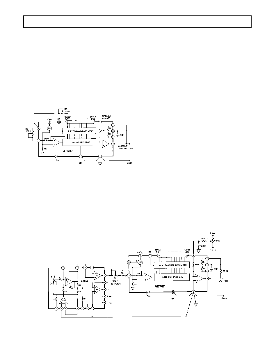
BIPOLAR CONFIGURATION (Figure 3)
This configuration will provide a bipolar output voltage from
–5.000 to +4.9976 volts, with positive full scale occurring with
all bits ON (all 1s).
STEP I … OFFSET ADJUST
Turn OFF all bits. Adjust 100
trimmer R1 to give –5.000
volts output.
STEP II … GAIN ADJUST
Turn ON all bits. Adjust 100
gain trimmer R2 to give a
reading of +4.9976 volts.
STEP III … BIPOLAR ZERO ADJUST (Optional)
In applications where an accurate zero output is required, set
the MSB ON, all other bits OFF, and readjust R1 for zero volts
output.
Figure 3.
±5 V Bipolar Voltage Output
INTERNAL/EXTERNAL REFERENCE USE
The AD767 has an internal low-noise buried Zener diode
reference which is trimmed for absolute accuracy and tempera-
ture coefficient. This reference is buffered and optimized for use
in a high-speed DAC and will give long-term stability equal or
superior to the best discrete Zener reference diodes. The per-
formance of the AD767 is specified with the internal reference
driving the DAC since all trimming and testing (especially for
full-scale error and bipolar offset) is done in this configuration.
The internal reference has sufficient buffering to drive external
circuitry in addition to the reference currents required for the
DAC (typically 0.5 mA to Ref In and 1.0 mA to Bipolar Offset).
A minimum of 0.1 mA is available for driving external loads.
The AD767 reference output should be buffered with an
external op amp if it is required to supply more than 0.1 mA
output current. The reference is typically trimmed to
±0.2%,
then tested and guaranteed to
±1.0% max error. The
temperature coefficient is comparable to that of the full-scale
TC for a particular grade.
If an external reference is used (10.000 V, for example),
additional trim range must be provided, since the internal
reference has a tolerance of
±1%, and the AD767 full-scale and
bipolar offset are both trimmed with the internal reference. The
gain and offset trim resistors give about
±0.25% adjustment
range, which is sufficient for the AD767 when used with the
internal reference.
It is also possible to use external references other than 10 volts.
The recommended range of reference voltage is from +8 to
+10.5 volts, which allows both 8.192 V and 10.24 V ranges to
be used. The AD767 is optimized for fixed-reference applications.
If the reference voltage is expected to vary over a wide range in
a particular application, a CMOS multiplying DAC is a better
choice.
Reduced values of reference voltage will also permit the
±12 volt
±5% power supply requirement to be relaxed to ±12 volts
±10%.
It is not recommended that the AD767 be used with external
feedback resistors to modify the scale factor. The internal
resistors are trimmed to ratio-match and temperature-track the
other resistors on the chip, even though their absolute tolerances
are
±20%, and absolute temperature coefficients are approximately
–50 ppm/
°C. If external resistors are used, a wide trim range
(
±20%) will be needed and temperature drift will be increased
to reflect the mismatch between the temperature coefficients of
the internal and external resistors.
Small resistors may be added to the feedback resistors in order
to accomplish small modifications in the scaling. For example, if
a 10.24 V full scale is desired, a 140
1% low-TC metal-film
resistor can be added in series with the internal (nominal) 5k
feedback resistor, and the gain trim potentiometer (between
Pins 6 and 7) should be increased to 200
. In the bipolar
mode, increase the value of the bipolar offset trim potentiometer
also to 200
.
Figure 4. Using the AD767 with the AD588 High Precision Reference
相关PDF资料 |
PDF描述 |
|---|---|
| LTC1597BCN#PBF | IC CONV D/A 16BIT PAR 28-DIP |
| AD7247ABRZ-REEL | IC DAC 12BIT AMP/BUFF 24SOIC |
| AD7237ABRZ-REEL | IC DAC 12BIT DUAL W/BUFF 24-SOIC |
| AD667KPZ-REEL | IC DAC 12BIT W/BUFF LATCH 28PLCC |
| VE-B6B-MW-B1 | CONVERTER MOD DC/DC 95V 100W |
相关代理商/技术参数 |
参数描述 |
|---|---|
| AD767JNZ | 功能描述:IC DAC 12BIT 24-DIP RoHS:是 类别:集成电路 (IC) >> 数据采集 - 数模转换器 系列:- 产品培训模块:Lead (SnPb) Finish for COTS Obsolescence Mitigation Program 标准包装:50 系列:- 设置时间:4µs 位数:12 数据接口:串行 转换器数目:2 电压电源:单电源 功率耗散(最大):- 工作温度:-40°C ~ 85°C 安装类型:表面贴装 封装/外壳:8-TSSOP,8-MSOP(0.118",3.00mm 宽) 供应商设备封装:8-uMAX 包装:管件 输出数目和类型:2 电压,单极 采样率(每秒):* 产品目录页面:1398 (CN2011-ZH PDF) |
| AD767JP | 功能描述:IC DAC 12BIT W/AMP 28-PLCC RoHS:否 类别:集成电路 (IC) >> 数据采集 - 数模转换器 系列:- 产品培训模块:Data Converter Fundamentals DAC Architectures 标准包装:750 系列:- 设置时间:7µs 位数:16 数据接口:并联 转换器数目:1 电压电源:双 ± 功率耗散(最大):100mW 工作温度:0°C ~ 70°C 安装类型:表面贴装 封装/外壳:28-LCC(J 形引线) 供应商设备封装:28-PLCC(11.51x11.51) 包装:带卷 (TR) 输出数目和类型:1 电压,单极;1 电压,双极 采样率(每秒):143k |
| AD767JP-REEL | 功能描述:IC DAC 12BIT W/AMP 28-PLCC RoHS:否 类别:集成电路 (IC) >> 数据采集 - 数模转换器 系列:- 产品培训模块:Data Converter Fundamentals DAC Architectures 标准包装:750 系列:- 设置时间:7µs 位数:16 数据接口:并联 转换器数目:1 电压电源:双 ± 功率耗散(最大):100mW 工作温度:0°C ~ 70°C 安装类型:表面贴装 封装/外壳:28-LCC(J 形引线) 供应商设备封装:28-PLCC(11.51x11.51) 包装:带卷 (TR) 输出数目和类型:1 电压,单极;1 电压,双极 采样率(每秒):143k |
| AD767JPZ | 功能描述:IC DAC 12BIT W/AMP 28-PLCC RoHS:是 类别:集成电路 (IC) >> 数据采集 - 数模转换器 系列:- 产品培训模块:Lead (SnPb) Finish for COTS Obsolescence Mitigation Program 标准包装:50 系列:- 设置时间:4µs 位数:12 数据接口:串行 转换器数目:2 电压电源:单电源 功率耗散(最大):- 工作温度:-40°C ~ 85°C 安装类型:表面贴装 封装/外壳:8-TSSOP,8-MSOP(0.118",3.00mm 宽) 供应商设备封装:8-uMAX 包装:管件 输出数目和类型:2 电压,单极 采样率(每秒):* 产品目录页面:1398 (CN2011-ZH PDF) |
| AD767JPZ-REEL | 功能描述:IC DAC 12BIT W/AMP 28-PLCC RoHS:是 类别:集成电路 (IC) >> 数据采集 - 数模转换器 系列:- 产品培训模块:Data Converter Fundamentals DAC Architectures 标准包装:750 系列:- 设置时间:7µs 位数:16 数据接口:并联 转换器数目:1 电压电源:双 ± 功率耗散(最大):100mW 工作温度:0°C ~ 70°C 安装类型:表面贴装 封装/外壳:28-LCC(J 形引线) 供应商设备封装:28-PLCC(11.51x11.51) 包装:带卷 (TR) 输出数目和类型:1 电压,单极;1 电压,双极 采样率(每秒):143k |
发布紧急采购,3分钟左右您将得到回复。