参数资料
| 型号: | AD767JN |
| 厂商: | Analog Devices Inc |
| 文件页数: | 7/8页 |
| 文件大小: | 0K |
| 描述: | IC DAC 12BIT 24-DIP |
| 产品培训模块: | Data Converter Fundamentals DAC Architectures |
| 标准包装: | 15 |
| 设置时间: | 3µs |
| 位数: | 12 |
| 数据接口: | 并联 |
| 转换器数目: | 1 |
| 电压电源: | 双 ± |
| 工作温度: | 0°C ~ 70°C |
| 安装类型: | 通孔 |
| 封装/外壳: | 24-DIP(0.300",7.62mm) |
| 供应商设备封装: | 24-PDIP |
| 包装: | 管件 |
| 输出数目和类型: | 1 电压,单极;1 电压,双极 |
| 采样率(每秒): | * |
AD767
REV. A
–7–
Figure 5e. Fine-Scale Settling, CF = 20 pF
DIGITAL INPUT CONSIDERATIONS
The threshold of the digital input circuitry is set at 1.4 volts and
does not change with supply voltage. Thus the AD767 digital
interface may be driven with any of the popular types of 5 volt
logic.
A good engineering practice is to connect unused inputs to
power ground to improve noise immunity. Unconnected data
and control inputs will float to logic 0 if left open.
The low digital input current of the AD767 eliminates the need
for buffer/drivers required by many monolithic converters using
bipolar technology. A single low-power Schottky gate, for
example, will drive several AD767s when connected to a
common bus.
INPUT CODING
The AD767 uses positive-true binary input coding. Logic “1” is
represented by an input voltage greater than 2.0 V, and logic
“0” is defined as an input voltage less than 0.8 V.
Unipolar coding is straight binary, where all zeroes (000H) on
the data inputs yields a zero analog output and all ones (FFFH)
yields an analog output 1 LSB below full scale.
Bipolar coding is offset binary, where an input code of 000H
yields a minus full-scale output, an input of FFFH yields an
output 1 LSB below positive full scale, and zero occurs for an
input code with only the MSB on (800H).
The AD767 can be used with twos complement input coding if
an inverter is used on the MSB (DB11).
MICROPROCESSOR INTERFACE
The AD767, with its 40 ns minimum CS pulse width, may be
easily interfaced to any of today’s high-speed microprocessors.
The 12-bit single buffered input register will accept 12-bit
parallel data from processors such as the 68000, 8086, TMS320
series, and the Analog Devices ADSP-2100. Several illustrative
examples follow.
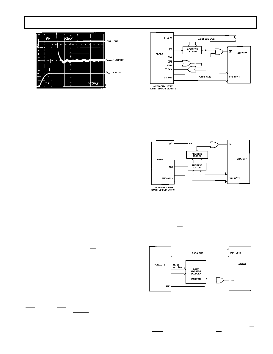
68000 – AD767 INTERFACE
Figure 6 illustrates the AD767 interface to a 68000 micro-
processor. An active low decoded address is OR’ed with the
processor’s R/W signal to provide CS and latch data into the
AD767. Later in the bus cycle the processor issues the upper
(UDS) and lower (LDS) data strobes which are gated with the
decoded address to provide DTACK and terminate the bus
cycle. As shown, this interface will support a 12.5 MHz 68000
system.
Figure 6. 68000 – AD767 Interface
8086 – AD767 INTERFACE
Interfacing the AD767 to the 8086 16-bit microprocessor
requires a minimal amount of external components. A 10 MHz
8086, for example, generates a 165 ns low write pulse which
may be gated with a decoded address to provide CS for the
AD767. As WR returns high valid data is latched into the DAC.
See Figure 7.
Figure 7. 8086 – AD767 Interface
TMS32010 – AD767 INTERFACE
The high-speed digital interface of the AD767 facilitates its use
with the TMS32010 microprocessor at speeds up to 20 MHz.
In the three multiplexed LSBs of the address bus, PA2 – PA0
are decoded as a port address and OR’ed with the low write
enable to generate CS for the DAC. A simple OUT xx,y
instruction will output the data word stored in memory location
xx to any one of eight port locations y.
Figure 8. TMS32010 – AD767 Interface
TMS32020 – AD767 INTERFACE
Interfacing the AD767 to the TMS32020 microprocessor is
easily achieved by using the TMS32020 I/O port capability. The
IS
signal distinguishes the I/O address space from the local
program/data memory space and is used to enable a 74LS138
decoder. The decoded port address is then gated with the R/W
and STRB signals to provide the AD767 CS.
相关PDF资料 |
PDF描述 |
|---|---|
| LTC1597BCN#PBF | IC CONV D/A 16BIT PAR 28-DIP |
| AD7247ABRZ-REEL | IC DAC 12BIT AMP/BUFF 24SOIC |
| AD7237ABRZ-REEL | IC DAC 12BIT DUAL W/BUFF 24-SOIC |
| AD667KPZ-REEL | IC DAC 12BIT W/BUFF LATCH 28PLCC |
| VE-B6B-MW-B1 | CONVERTER MOD DC/DC 95V 100W |
相关代理商/技术参数 |
参数描述 |
|---|---|
| AD767JNZ | 功能描述:IC DAC 12BIT 24-DIP RoHS:是 类别:集成电路 (IC) >> 数据采集 - 数模转换器 系列:- 产品培训模块:Lead (SnPb) Finish for COTS Obsolescence Mitigation Program 标准包装:50 系列:- 设置时间:4µs 位数:12 数据接口:串行 转换器数目:2 电压电源:单电源 功率耗散(最大):- 工作温度:-40°C ~ 85°C 安装类型:表面贴装 封装/外壳:8-TSSOP,8-MSOP(0.118",3.00mm 宽) 供应商设备封装:8-uMAX 包装:管件 输出数目和类型:2 电压,单极 采样率(每秒):* 产品目录页面:1398 (CN2011-ZH PDF) |
| AD767JP | 功能描述:IC DAC 12BIT W/AMP 28-PLCC RoHS:否 类别:集成电路 (IC) >> 数据采集 - 数模转换器 系列:- 产品培训模块:Data Converter Fundamentals DAC Architectures 标准包装:750 系列:- 设置时间:7µs 位数:16 数据接口:并联 转换器数目:1 电压电源:双 ± 功率耗散(最大):100mW 工作温度:0°C ~ 70°C 安装类型:表面贴装 封装/外壳:28-LCC(J 形引线) 供应商设备封装:28-PLCC(11.51x11.51) 包装:带卷 (TR) 输出数目和类型:1 电压,单极;1 电压,双极 采样率(每秒):143k |
| AD767JP-REEL | 功能描述:IC DAC 12BIT W/AMP 28-PLCC RoHS:否 类别:集成电路 (IC) >> 数据采集 - 数模转换器 系列:- 产品培训模块:Data Converter Fundamentals DAC Architectures 标准包装:750 系列:- 设置时间:7µs 位数:16 数据接口:并联 转换器数目:1 电压电源:双 ± 功率耗散(最大):100mW 工作温度:0°C ~ 70°C 安装类型:表面贴装 封装/外壳:28-LCC(J 形引线) 供应商设备封装:28-PLCC(11.51x11.51) 包装:带卷 (TR) 输出数目和类型:1 电压,单极;1 电压,双极 采样率(每秒):143k |
| AD767JPZ | 功能描述:IC DAC 12BIT W/AMP 28-PLCC RoHS:是 类别:集成电路 (IC) >> 数据采集 - 数模转换器 系列:- 产品培训模块:Lead (SnPb) Finish for COTS Obsolescence Mitigation Program 标准包装:50 系列:- 设置时间:4µs 位数:12 数据接口:串行 转换器数目:2 电压电源:单电源 功率耗散(最大):- 工作温度:-40°C ~ 85°C 安装类型:表面贴装 封装/外壳:8-TSSOP,8-MSOP(0.118",3.00mm 宽) 供应商设备封装:8-uMAX 包装:管件 输出数目和类型:2 电压,单极 采样率(每秒):* 产品目录页面:1398 (CN2011-ZH PDF) |
| AD767JPZ-REEL | 功能描述:IC DAC 12BIT W/AMP 28-PLCC RoHS:是 类别:集成电路 (IC) >> 数据采集 - 数模转换器 系列:- 产品培训模块:Data Converter Fundamentals DAC Architectures 标准包装:750 系列:- 设置时间:7µs 位数:16 数据接口:并联 转换器数目:1 电压电源:双 ± 功率耗散(最大):100mW 工作温度:0°C ~ 70°C 安装类型:表面贴装 封装/外壳:28-LCC(J 形引线) 供应商设备封装:28-PLCC(11.51x11.51) 包装:带卷 (TR) 输出数目和类型:1 电压,单极;1 电压,双极 采样率(每秒):143k |
发布紧急采购,3分钟左右您将得到回复。