参数资料
| 型号: | AD767JN |
| 厂商: | Analog Devices Inc |
| 文件页数: | 6/8页 |
| 文件大小: | 0K |
| 描述: | IC DAC 12BIT 24-DIP |
| 产品培训模块: | Data Converter Fundamentals DAC Architectures |
| 标准包装: | 15 |
| 设置时间: | 3µs |
| 位数: | 12 |
| 数据接口: | 并联 |
| 转换器数目: | 1 |
| 电压电源: | 双 ± |
| 工作温度: | 0°C ~ 70°C |
| 安装类型: | 通孔 |
| 封装/外壳: | 24-DIP(0.300",7.62mm) |
| 供应商设备封装: | 24-PDIP |
| 包装: | 管件 |
| 输出数目和类型: | 1 电压,单极;1 电压,双极 |
| 采样率(每秒): | * |
AD767
REV. A
–6–
USING THE AD767 WITH THE AD588 HIGH PRECISION
VOLTAGE REFERENCE
The AD767 is specified for gain drift from 15 ppm/
°C to
30 ppm/
°C (depending on grade) using its internal 10 volt
reference. Since the internal reference contributes the majority
of this drift, an external high-precision voltage reference will
greatly improve performance over temperature. As shown in
Figure 4, the 10 volt output from the AD588 is used as the
reference. With a 1.5 ppm/
°C output voltage drift the AD588
contributes less than 1/2 LSB gain drift when used with the
AD767 over the industrial temperature range. Using this
combination may result in apparent increases in full-scale error
due to the differences between the internal reference by which
the device is laser trimmed and the external reference with
which the device is actually applied. The AD767 internal
reference is specified to be 10 volts
±100 mV whereas the
AD588 is specified as 10 volts
±1 mV. This may result in up to
101 mV of apparent full-scale error beyond the
±25 mV
specified AD767 gain error. The 500
potentiometer in series
with the reference input allows adequate trim range to null this
error.
GROUNDING RULES
The AD767 brings out separate analog and power grounds to
allow optimum connections for low noise and high-speed
performance. These grounds should be tied together at one
point, usually the device power ground. The separate ground
returns are provided to minimize current flow in low-level signal
paths.
The analog ground at Pin 5 is the ground point for the output
amplifier and is thus the “high quality” ground for the AD767;
it should be connected directly to the analog reference point of
the system. The power ground at Pin 12 can be connected to
the most convenient ground point; analog power return is
preferred. If power ground contains high frequency noise
beyond 200 mV, this noise may feed through the converter, thus
some caution will be required in applying these grounds.
It is also important to apply decoupling capacitors properly on
the power supplies for the AD767. The correct method for
decoupling is to connect a capacitor from each power supply pin
of the AD767 to the analog ground pin of the AD767. Any load
driven by the output amplifier should also be referred to the
analog ground pin.
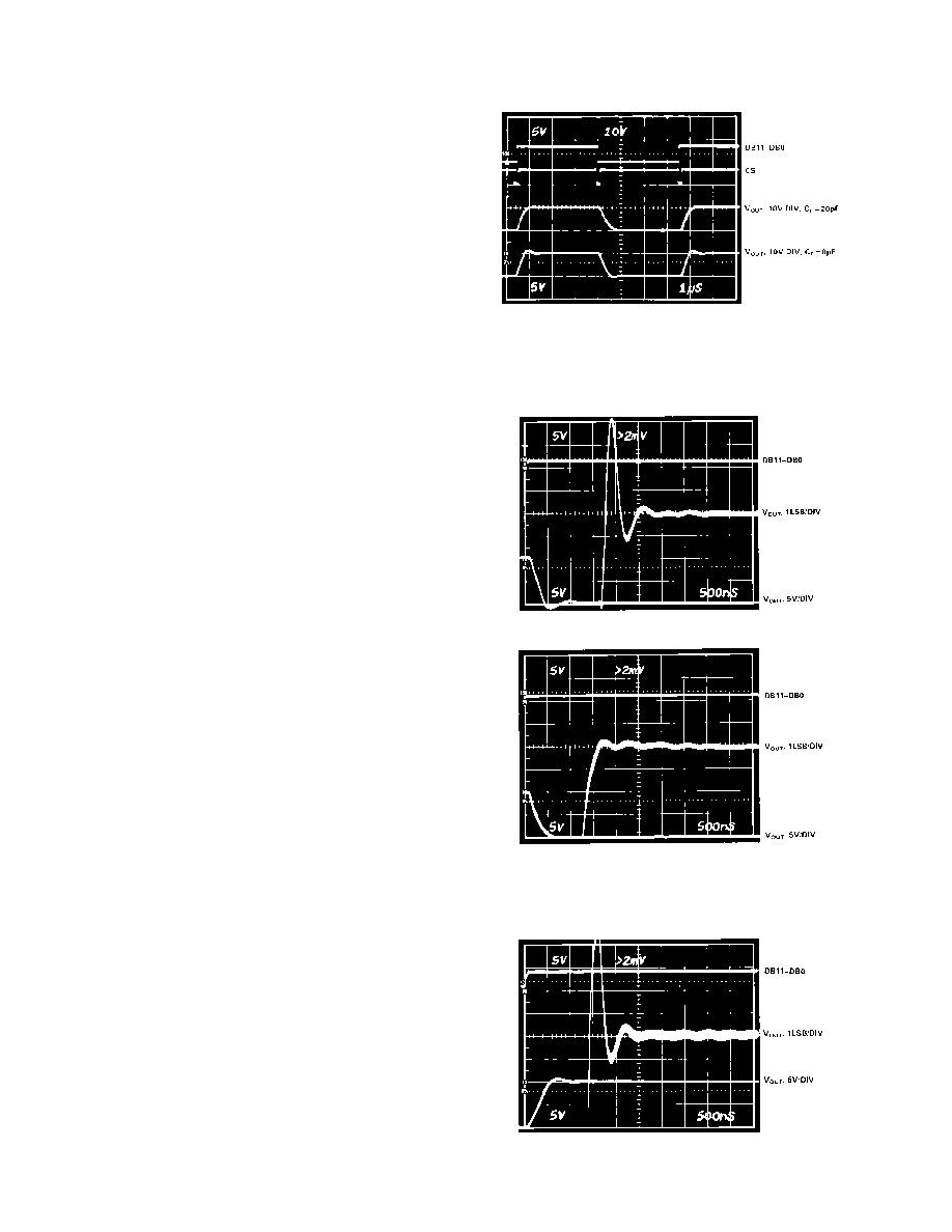
OPTIMIZING SETTLING TIME
The dynamic performance of the AD767’s output amplifier can
be optimized by adding a small (20 pF) capacitor across the
feedback resistor. Figure 5 shows the improvement in both
large-signal and small-signal settling for the 10 V range. In
Figure 5a, the top trace shows the data inputs (DB11–DB0 tied
together), the second trace shows the CS pulse, and the lower
two traces show the analog outputs for CF = 0 and 20 pF
respectively.
Figure 5a. Large Scale Settling
Figures 5b and 5c show the settling time for the transition from
all bits on to all bits off. Note that the settling time to
±1/2 LSB
for the 10 V step is improved from 2.4 microseconds to 1.6
microseconds by the addition of the 20 pF capacitor.
Figure 5b. Fine-Scale Settling, CF = 0 pF
Figure 5c. Fine-Scale Settling, CF = 20 pF
Figures 5d and 5e show the settling time for the transition from
all bits off to all bits on. The improvement in settling time
gained by adding CC = 20 pF is similar.
Figure 5d. Fine-Scale Settling, CF = 0 pF
相关PDF资料 |
PDF描述 |
|---|---|
| LTC1597BCN#PBF | IC CONV D/A 16BIT PAR 28-DIP |
| AD7247ABRZ-REEL | IC DAC 12BIT AMP/BUFF 24SOIC |
| AD7237ABRZ-REEL | IC DAC 12BIT DUAL W/BUFF 24-SOIC |
| AD667KPZ-REEL | IC DAC 12BIT W/BUFF LATCH 28PLCC |
| VE-B6B-MW-B1 | CONVERTER MOD DC/DC 95V 100W |
相关代理商/技术参数 |
参数描述 |
|---|---|
| AD767JNZ | 功能描述:IC DAC 12BIT 24-DIP RoHS:是 类别:集成电路 (IC) >> 数据采集 - 数模转换器 系列:- 产品培训模块:Lead (SnPb) Finish for COTS Obsolescence Mitigation Program 标准包装:50 系列:- 设置时间:4µs 位数:12 数据接口:串行 转换器数目:2 电压电源:单电源 功率耗散(最大):- 工作温度:-40°C ~ 85°C 安装类型:表面贴装 封装/外壳:8-TSSOP,8-MSOP(0.118",3.00mm 宽) 供应商设备封装:8-uMAX 包装:管件 输出数目和类型:2 电压,单极 采样率(每秒):* 产品目录页面:1398 (CN2011-ZH PDF) |
| AD767JP | 功能描述:IC DAC 12BIT W/AMP 28-PLCC RoHS:否 类别:集成电路 (IC) >> 数据采集 - 数模转换器 系列:- 产品培训模块:Data Converter Fundamentals DAC Architectures 标准包装:750 系列:- 设置时间:7µs 位数:16 数据接口:并联 转换器数目:1 电压电源:双 ± 功率耗散(最大):100mW 工作温度:0°C ~ 70°C 安装类型:表面贴装 封装/外壳:28-LCC(J 形引线) 供应商设备封装:28-PLCC(11.51x11.51) 包装:带卷 (TR) 输出数目和类型:1 电压,单极;1 电压,双极 采样率(每秒):143k |
| AD767JP-REEL | 功能描述:IC DAC 12BIT W/AMP 28-PLCC RoHS:否 类别:集成电路 (IC) >> 数据采集 - 数模转换器 系列:- 产品培训模块:Data Converter Fundamentals DAC Architectures 标准包装:750 系列:- 设置时间:7µs 位数:16 数据接口:并联 转换器数目:1 电压电源:双 ± 功率耗散(最大):100mW 工作温度:0°C ~ 70°C 安装类型:表面贴装 封装/外壳:28-LCC(J 形引线) 供应商设备封装:28-PLCC(11.51x11.51) 包装:带卷 (TR) 输出数目和类型:1 电压,单极;1 电压,双极 采样率(每秒):143k |
| AD767JPZ | 功能描述:IC DAC 12BIT W/AMP 28-PLCC RoHS:是 类别:集成电路 (IC) >> 数据采集 - 数模转换器 系列:- 产品培训模块:Lead (SnPb) Finish for COTS Obsolescence Mitigation Program 标准包装:50 系列:- 设置时间:4µs 位数:12 数据接口:串行 转换器数目:2 电压电源:单电源 功率耗散(最大):- 工作温度:-40°C ~ 85°C 安装类型:表面贴装 封装/外壳:8-TSSOP,8-MSOP(0.118",3.00mm 宽) 供应商设备封装:8-uMAX 包装:管件 输出数目和类型:2 电压,单极 采样率(每秒):* 产品目录页面:1398 (CN2011-ZH PDF) |
| AD767JPZ-REEL | 功能描述:IC DAC 12BIT W/AMP 28-PLCC RoHS:是 类别:集成电路 (IC) >> 数据采集 - 数模转换器 系列:- 产品培训模块:Data Converter Fundamentals DAC Architectures 标准包装:750 系列:- 设置时间:7µs 位数:16 数据接口:并联 转换器数目:1 电压电源:双 ± 功率耗散(最大):100mW 工作温度:0°C ~ 70°C 安装类型:表面贴装 封装/外壳:28-LCC(J 形引线) 供应商设备封装:28-PLCC(11.51x11.51) 包装:带卷 (TR) 输出数目和类型:1 电压,单极;1 电压,双极 采样率(每秒):143k |
发布紧急采购,3分钟左右您将得到回复。