参数资料
| 型号: | AD767JN |
| 厂商: | Analog Devices Inc |
| 文件页数: | 8/8页 |
| 文件大小: | 0K |
| 描述: | IC DAC 12BIT 24-DIP |
| 产品培训模块: | Data Converter Fundamentals DAC Architectures |
| 标准包装: | 15 |
| 设置时间: | 3µs |
| 位数: | 12 |
| 数据接口: | 并联 |
| 转换器数目: | 1 |
| 电压电源: | 双 ± |
| 工作温度: | 0°C ~ 70°C |
| 安装类型: | 通孔 |
| 封装/外壳: | 24-DIP(0.300",7.62mm) |
| 供应商设备封装: | 24-PDIP |
| 包装: | 管件 |
| 输出数目和类型: | 1 电压,单极;1 电压,双极 |
| 采样率(每秒): | * |
AD767
REV. A
–8–
C1068a–10–4/88
PRINTED
IN
U.S.A.
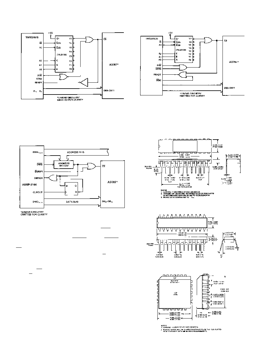
Figure 9. TMS32020 – AD767 Interface
ADSP-2100 – AD767 INTERFACE
The ADSP-2100 single chip DSP processor may be interfaced
to the AD767 as shown in Figure 10. With a clock frequency of
32 MHz, and instruction execution in a single 125 ns cycle, the
processor will support the AD767 interface with a single wait
state.
Figure 10. ADSP-2100 – AD767 Interface
At the beginning of the data memory access cycle the processor
provides a 14-bit address on the DMA bus. The DMS signal is
then asserted enabling a LOW address decode. Valid data is
now placed on the data bus and DMWR is issued. DMWR is
OR’ed with the LOW address decode to generate the AD767
CS
.
The LOW decoded address is also gated with the Q output of a
D flip-flop to hold DMACK (Data Memory Acknowledge)
LOW. This forces the processor into a wait state and extends
the AD767 CS by 1 clock cycle. The rising edge of CLKOUT
latches Q HIGH bringing DMACK HIGH. The cycle is now
complete.
TMS320C25 – AD767 INTERFACE
Figure 11 illustrates the AD767 interface to a TMS320C25
digital signal processor. Due to the high-speed capability of the
processor (40 MHz), a single wait state is required and is easily
generated using MSC. A 20 MHz TMS320C25 however, does
not require wait states and should be interfaced using the circuit
shown in Figure 9.
Figure 11. TMS320C25 – AD767 Interface
OUTLINE DIMENSIONS
Dimensions shown in inches and (mm).
24-Pin Ceramic (Suffix D)
24-Pin Plastic (Suffix N)
28-Pin PLCC (Suffix P)
相关PDF资料 |
PDF描述 |
|---|---|
| LTC1597BCN#PBF | IC CONV D/A 16BIT PAR 28-DIP |
| AD7247ABRZ-REEL | IC DAC 12BIT AMP/BUFF 24SOIC |
| AD7237ABRZ-REEL | IC DAC 12BIT DUAL W/BUFF 24-SOIC |
| AD667KPZ-REEL | IC DAC 12BIT W/BUFF LATCH 28PLCC |
| VE-B6B-MW-B1 | CONVERTER MOD DC/DC 95V 100W |
相关代理商/技术参数 |
参数描述 |
|---|---|
| AD767JNZ | 功能描述:IC DAC 12BIT 24-DIP RoHS:是 类别:集成电路 (IC) >> 数据采集 - 数模转换器 系列:- 产品培训模块:Lead (SnPb) Finish for COTS Obsolescence Mitigation Program 标准包装:50 系列:- 设置时间:4µs 位数:12 数据接口:串行 转换器数目:2 电压电源:单电源 功率耗散(最大):- 工作温度:-40°C ~ 85°C 安装类型:表面贴装 封装/外壳:8-TSSOP,8-MSOP(0.118",3.00mm 宽) 供应商设备封装:8-uMAX 包装:管件 输出数目和类型:2 电压,单极 采样率(每秒):* 产品目录页面:1398 (CN2011-ZH PDF) |
| AD767JP | 功能描述:IC DAC 12BIT W/AMP 28-PLCC RoHS:否 类别:集成电路 (IC) >> 数据采集 - 数模转换器 系列:- 产品培训模块:Data Converter Fundamentals DAC Architectures 标准包装:750 系列:- 设置时间:7µs 位数:16 数据接口:并联 转换器数目:1 电压电源:双 ± 功率耗散(最大):100mW 工作温度:0°C ~ 70°C 安装类型:表面贴装 封装/外壳:28-LCC(J 形引线) 供应商设备封装:28-PLCC(11.51x11.51) 包装:带卷 (TR) 输出数目和类型:1 电压,单极;1 电压,双极 采样率(每秒):143k |
| AD767JP-REEL | 功能描述:IC DAC 12BIT W/AMP 28-PLCC RoHS:否 类别:集成电路 (IC) >> 数据采集 - 数模转换器 系列:- 产品培训模块:Data Converter Fundamentals DAC Architectures 标准包装:750 系列:- 设置时间:7µs 位数:16 数据接口:并联 转换器数目:1 电压电源:双 ± 功率耗散(最大):100mW 工作温度:0°C ~ 70°C 安装类型:表面贴装 封装/外壳:28-LCC(J 形引线) 供应商设备封装:28-PLCC(11.51x11.51) 包装:带卷 (TR) 输出数目和类型:1 电压,单极;1 电压,双极 采样率(每秒):143k |
| AD767JPZ | 功能描述:IC DAC 12BIT W/AMP 28-PLCC RoHS:是 类别:集成电路 (IC) >> 数据采集 - 数模转换器 系列:- 产品培训模块:Lead (SnPb) Finish for COTS Obsolescence Mitigation Program 标准包装:50 系列:- 设置时间:4µs 位数:12 数据接口:串行 转换器数目:2 电压电源:单电源 功率耗散(最大):- 工作温度:-40°C ~ 85°C 安装类型:表面贴装 封装/外壳:8-TSSOP,8-MSOP(0.118",3.00mm 宽) 供应商设备封装:8-uMAX 包装:管件 输出数目和类型:2 电压,单极 采样率(每秒):* 产品目录页面:1398 (CN2011-ZH PDF) |
| AD767JPZ-REEL | 功能描述:IC DAC 12BIT W/AMP 28-PLCC RoHS:是 类别:集成电路 (IC) >> 数据采集 - 数模转换器 系列:- 产品培训模块:Data Converter Fundamentals DAC Architectures 标准包装:750 系列:- 设置时间:7µs 位数:16 数据接口:并联 转换器数目:1 电压电源:双 ± 功率耗散(最大):100mW 工作温度:0°C ~ 70°C 安装类型:表面贴装 封装/外壳:28-LCC(J 形引线) 供应商设备封装:28-PLCC(11.51x11.51) 包装:带卷 (TR) 输出数目和类型:1 电压,单极;1 电压,双极 采样率(每秒):143k |
发布紧急采购,3分钟左右您将得到回复。