- 您现在的位置:买卖IC网 > PDF目录10228 > AD7685CRMZRL7 (Analog Devices Inc)IC ADC 16BIT PSEUDO-DIFF 10MSOP PDF资料下载
参数资料
| 型号: | AD7685CRMZRL7 |
| 厂商: | Analog Devices Inc |
| 文件页数: | 13/28页 |
| 文件大小: | 0K |
| 描述: | IC ADC 16BIT PSEUDO-DIFF 10MSOP |
| 产品培训模块: | Power Line Monitoring Motor Control |
| 设计资源: | Parametric Measurement Unit and Supporting Components for PAD Appls Using AD5522 and AD7685 (CN0104) Integrated Device Power Supply for PAD with Output Voltage Range 0 V to 25 V (CN0130) |
| 标准包装: | 1,000 |
| 系列: | PulSAR® |
| 位数: | 16 |
| 采样率(每秒): | 250k |
| 数据接口: | DSP,MICROWIRE?,QSPI?,串行,SPI? |
| 转换器数目: | 1 |
| 功率耗散(最大): | 15mW |
| 电压电源: | 模拟和数字 |
| 工作温度: | -40°C ~ 85°C |
| 安装类型: | 表面贴装 |
| 封装/外壳: | 10-TFSOP,10-MSOP(0.118",3.00mm 宽) |
| 供应商设备封装: | 10-MSOP |
| 包装: | 带卷 (TR) |
| 输入数目和类型: | 1 个伪差分,单极 |
| 配用: | EVAL-AD7685CBZ-ND - BOARD EVAL FOR AD7685 |
第1页第2页第3页第4页第5页第6页第7页第8页第9页第10页第11页第12页当前第13页第14页第15页第16页第17页第18页第19页第20页第21页第22页第23页第24页第25页第26页第27页第28页
AD7685
Rev. C | Page 20 of 28
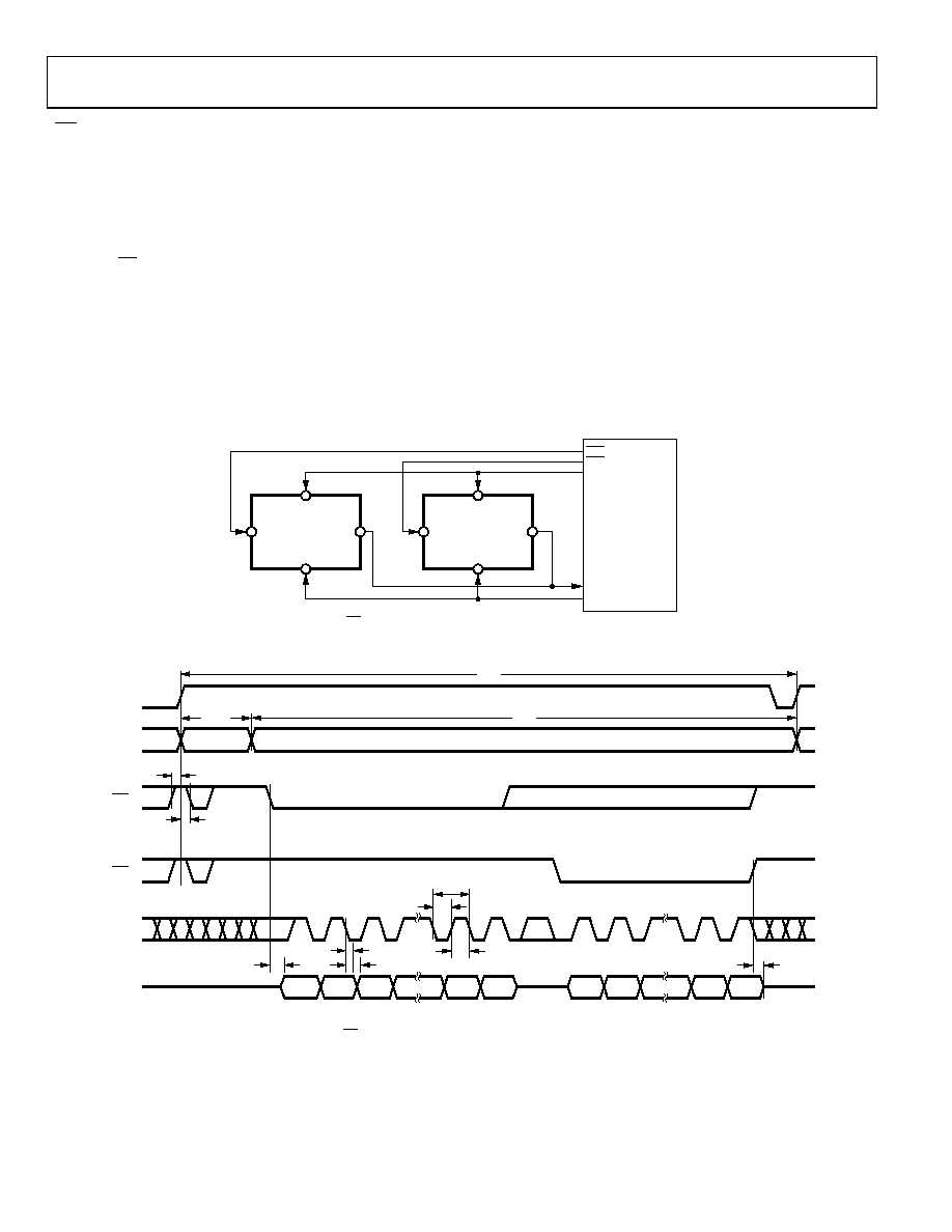
CS MODE 4-WIRE, NO BUSY INDICATOR
This mode is usually used when multiple AD7685s are
connected to an SPI-compatible digital host.
A connection diagram example using two AD7685s is shown in
With SDI high, a rising edge on CNV initiates a conversion,
selects the CS mode, and forces SDO to high impedance. In this
mode, CNV must be held high during the conversion phase and
the subsequent data readback (if SDI and CNV are low, SDO is
driven low). Prior to the minimum conversion time, SDI could
be used to select other SPI devices, such as analog multiplexers,
but SDI must be returned high before the minimum conversion
time and held high until the maximum conversion time to
avoid the generation of the BUSY signal indicator. When the
conversion is complete, the AD7685 enters the acquisition
phase and powers down. Each ADC result can be read by
bringing low its SDI input, which consequently outputs the
MSB onto SDO. The remaining data bits are then clocked by
subsequent SCK falling edges. The data is valid on both SCK
edges. Although the rising edge can be used to capture the data,
a digital host using the SCK falling edge will allow a faster
reading rate, provided it has an acceptable hold time. After the
16th SCK falling edge, or when SDI goes high, whichever is
earlier, SDO returns to high impedance and another AD7685
can be read.
If multiple AD7685s are selected at the same time, the SDO
output pin handles this contention without damage or induced
latch-up. Meanwhile, it is recommended to keep this contention
as short as possible to limit extra power dissipation.
DATA IN
CLK
CS1
CONVERT
CS2
DIGITAL HOST
02
96
8-
0
3
6
CNV
SCK
SDO
SDI
AD7685
CNV
SCK
SDO
SDI
AD7685
Figure 38. CS Mode 4-Wire, No BUSY Indicator Connection Diagram
SDO
D15
D14
D13
D1
D0
tDIS
SCK
12
3
30
31
32
tHSDO
tDSDO
tEN
CONVERSION
ACQUISITION
tCONV
tCYC
tACQ
ACQUISITION
SDI(CS1)
CNV
tSSDICNV
tHSDICNV
D1
14
15
tSCK
tSCKL
tSCKH
D0
D15
D14
17
18
16
SDI(CS2)
02
96
8-
03
7
Figure 39. CS Mode 4-Wire, No BUSY Indicator Serial Interface Timing
相关PDF资料 |
PDF描述 |
|---|---|
| ADM4852ARZ-REEL7 | IC TXRX RS485/422 2.5MBPS 8SOIC |
| AD7714ARSZ-3REEL | IC ADC 24BIT SIGMA-DELTA 28SSOP |
| SP490CN-L/TR | IC TXRX RS485 FULL DUPLEX 8NSOIC |
| SP1485EMN-L/TR | IC TXRX RS485 DIFF ESD 8SOIC |
| LTC1745IFW#PBF | IC ADC 12BIT 25MSPS LN 48TSSOP |
相关代理商/技术参数 |
参数描述 |
|---|---|
| AD7685-C-U2 | 制造商:Analog Devices 功能描述:250 KSPS 16-BIT PULSAR? A/D CONVERTER IN ?SOIC - Bulk |
| AD7685-S-U2 | 制造商:Analog Devices 功能描述:250 KSPS 16-BIT PULSAR? A/D CONVERTER - Bulk |
| AD7685XRM-U3 | 制造商:Analog Devices 功能描述:A/D CONVERTER 250KSPS 16-BIT PULSAR - Bulk |
| AD7686 | 制造商:AD 制造商全称:Analog Devices 功能描述:16-Bit, +/-0.65 LSB INL, 500 kSPS PulSAR Differential ADC in MSOP/QFN |
| AD76861 | 制造商:AD 制造商全称:Analog Devices 功能描述:18-Bit, 2 MSPS PulSAR 15 mW ADC in LFCSP (QFN) |
发布紧急采购,3分钟左右您将得到回复。