参数资料
| 型号: | AD7710AQ |
| 厂商: | Analog Devices Inc |
| 文件页数: | 16/32页 |
| 文件大小: | 0K |
| 描述: | IC ADC 24BIT DIFF INP 24-CDIP |
| 标准包装: | 15 |
| 位数: | 24 |
| 采样率(每秒): | 1.03k |
| 数据接口: | 串行 |
| 转换器数目: | 1 |
| 功率耗散(最大): | 45mW |
| 电压电源: | 模拟和数字,双 ± |
| 工作温度: | -40°C ~ 85°C |
| 安装类型: | 通孔 |
| 封装/外壳: | 24-CDIP(0.300",7.62mm) |
| 供应商设备封装: | 24-CDIP |
| 包装: | 管件 |
| 输入数目和类型: | 2 个差分,单极;2 个差分,双极 |
第1页第2页第3页第4页第5页第6页第7页第8页第9页第10页第11页第12页第13页第14页第15页当前第16页第17页第18页第19页第20页第21页第22页第23页第24页第25页第26页第27页第28页第29页第30页第31页第32页
AD7710
REV. G
–23–
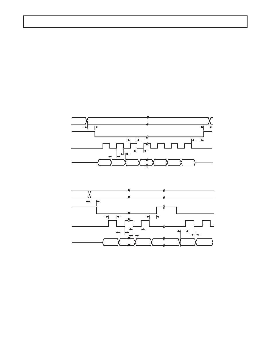
Write Operation
Data can be written to either the control register or calibration
registers. In either case, the write operation is not affected by
the
DRDY line and does not have any effect on the status of
DRDY. A write operation to the control register or the calibra-
tion register must always write 24 bits.
Figure 13a shows a write operation to the AD7710 with
TFS
remaining low for the duration of the operation. A0 determines
whether a write operation transfers data to the control register
or to the calibration registers. This A0 signal must remain valid
for the duration of the serial write operation. As before, the
serial clock line should be low between read and write opera-
tions. The serial data to be loaded to the AD7710 must be valid
on the high level of the externally applied SCLK signal. Data is
clocked into the AD7710 on the high level of this SCLK signal
with the MSB transferred first. On the last active high time of
SCLK, the LSB is loaded to the AD7710.
Figure 13b shows a timing diagram for a write operation to the
AD7710 with
TFS returning high during the operation and
returning low again to write the rest of the data-word. Timing
parameters and functions are very similar to those outlined for
Figure 13a, but Figure 13b has a number of additional times to
show timing relationships when
TFS returns high in the middle
of transferring a word.
Data to be loaded to the AD7710 must be valid prior to the
rising edge of the SCLK signal.
TFS should return high during
the low time of SCLK. After
TFS returns low again, the next bit
of the data-word to be loaded to the AD7710 is clocked in on
next high level of the SCLK input. On the last active high time
of the SCLK input, the LSB is loaded to the AD7710.
t35
t33
SCLK (I)
SDATA (I)
A0 (I)
t32
MSB
LSB
t26
t27
t34
TFS (I)
t36
Figure 13a. External Clocking Mode, Control/Calibration Register Write Operation
t35
SCLK (I)
SDATA (I)
TFS (I)
A0 (I)
MSB
BIT N
BIT N+1
t32
t26
t30
t27
t36
t35
t36
Figure 13b. External Clocking Mode, Control/Calibration Register Write Operation
(
TFS Returns High during Write Operation)
相关PDF资料 |
PDF描述 |
|---|---|
| AD7711AAR | IC ADC 24BIT RTD I SOURCE 24SOIC |
| AD7711AN | IC ADC 24BIT RTD I SOURCE 24-DIP |
| AD7712AR | IC ADC SIGNAL COND LC2MOS 24SOIC |
| AD7713AN | IC ADC 24BIT SIGMA-DELTA 24-DIP |
| AD7714ARS-3 | IC ADC 24BIT SIGMA-DELTA 28SSOP |
相关代理商/技术参数 |
参数描述 |
|---|---|
| AD7710AR | 功能描述:IC ADC 24BIT DIFF INP 24-SOIC RoHS:否 类别:集成电路 (IC) >> 数据采集 - 模数转换器 系列:- 标准包装:1 系列:- 位数:14 采样率(每秒):83k 数据接口:串行,并联 转换器数目:1 功率耗散(最大):95mW 电压电源:双 ± 工作温度:0°C ~ 70°C 安装类型:通孔 封装/外壳:28-DIP(0.600",15.24mm) 供应商设备封装:28-PDIP 包装:管件 输入数目和类型:1 个单端,双极 |
| AD7710AR-REEL | 功能描述:IC ADC 24BIT DIFF INP 24-SOIC RoHS:否 类别:集成电路 (IC) >> 数据采集 - 模数转换器 系列:- 标准包装:1 系列:- 位数:14 采样率(每秒):83k 数据接口:串行,并联 转换器数目:1 功率耗散(最大):95mW 电压电源:双 ± 工作温度:0°C ~ 70°C 安装类型:通孔 封装/外壳:28-DIP(0.600",15.24mm) 供应商设备封装:28-PDIP 包装:管件 输入数目和类型:1 个单端,双极 |
| AD7710AR-REEL7 | 功能描述:IC ADC 24BIT DIFF INP 24-SOIC RoHS:否 类别:集成电路 (IC) >> 数据采集 - 模数转换器 系列:- 标准包装:1 系列:- 位数:14 采样率(每秒):83k 数据接口:串行,并联 转换器数目:1 功率耗散(最大):95mW 电压电源:双 ± 工作温度:0°C ~ 70°C 安装类型:通孔 封装/外壳:28-DIP(0.600",15.24mm) 供应商设备封装:28-PDIP 包装:管件 输入数目和类型:1 个单端,双极 |
| AD7710ARZ | 功能描述:IC ADC 24BIT DIFF INP 24-SOIC RoHS:是 类别:集成电路 (IC) >> 数据采集 - 模数转换器 系列:- 标准包装:1 系列:microPOWER™ 位数:8 采样率(每秒):1M 数据接口:串行,SPI? 转换器数目:1 功率耗散(最大):- 电压电源:模拟和数字 工作温度:-40°C ~ 125°C 安装类型:表面贴装 封装/外壳:24-VFQFN 裸露焊盘 供应商设备封装:24-VQFN 裸露焊盘(4x4) 包装:Digi-Reel® 输入数目和类型:8 个单端,单极 产品目录页面:892 (CN2011-ZH PDF) 其它名称:296-25851-6 |
| AD7710ARZ | 制造商:Analog Devices 功能描述:IC ADC 24BIT 1.02KSPS SOIC-24 |
发布紧急采购,3分钟左右您将得到回复。