- 您现在的位置:买卖IC网 > PDF目录10245 > AD7739BRUZ-REEL7 (Analog Devices Inc)IC ADC 24BIT 8CH SIG-DEL 24TSSOP PDF资料下载
参数资料
| 型号: | AD7739BRUZ-REEL7 |
| 厂商: | Analog Devices Inc |
| 文件页数: | 3/32页 |
| 文件大小: | 0K |
| 描述: | IC ADC 24BIT 8CH SIG-DEL 24TSSOP |
| 标准包装: | 1,000 |
| 位数: | 24 |
| 采样率(每秒): | 15.1k |
| 数据接口: | DSP,MICROWIRE?,QSPI?,串行,SPI? |
| 转换器数目: | 1 |
| 功率耗散(最大): | 100mW |
| 电压电源: | 模拟和数字 |
| 工作温度: | -40°C ~ 105°C |
| 安装类型: | 表面贴装 |
| 封装/外壳: | 24-TSSOP(0.173",4.40mm 宽) |
| 供应商设备封装: | 24-TSSOP |
| 包装: | 带卷 (TR) |
| 输入数目和类型: | 8 个单端,单极;8 个单端,双极;4 个差分,单极;4 个差分,双极 |
| 配用: | EVAL-AD7739EBZ-ND - BOARD EVAL FOR AD7739 |
第1页第2页当前第3页第4页第5页第6页第7页第8页第9页第10页第11页第12页第13页第14页第15页第16页第17页第18页第19页第20页第21页第22页第23页第24页第25页第26页第27页第28页第29页第30页第31页第32页
Data Sheet
AD7739
Rev. A | Page 11 of 32
OUTPUT NOISE AND RESOLUTION SPECIFICATION
The AD7739 can be operated with chopping enabled or
disabled, allowing the ADC to be programmed to optimize
either the offset drift performance or the throughput rate and
channel switching time. Noise tables for these two primary
modes of operation are outlined below for a selection of output
rates and settling times.
The AD7739 noise performance depends on the selected
chopping mode, the filter word (FW) value, and the selected
analog input range. The AD7739 noise does not vary
significantly with MCLK frequency.
CHOPPING ENABLED
The first mode, in which the AD7739 is configured with
chopping enabled (chop = 1), provides very low noise with
lower output rates.
performance versus the channel conversion time and equivalent
output data rate, respectively.
typical effective resolution based on rms noise. Table 7 shows
the typical output peak-to-peak resolution, representing values
for which there is no code flicker within a 6-sigma limit. The
peak-to-peak resolutions are not calculated based on rms noise
but on peak-to-peak noise.
These typical numbers are generated from 4096 data samples
acquired in continuous conversion mode with an analog input
voltage set to 0 V and MCLK = 6.144 MHz. The conversion
time is selected via the channel conversion time register.
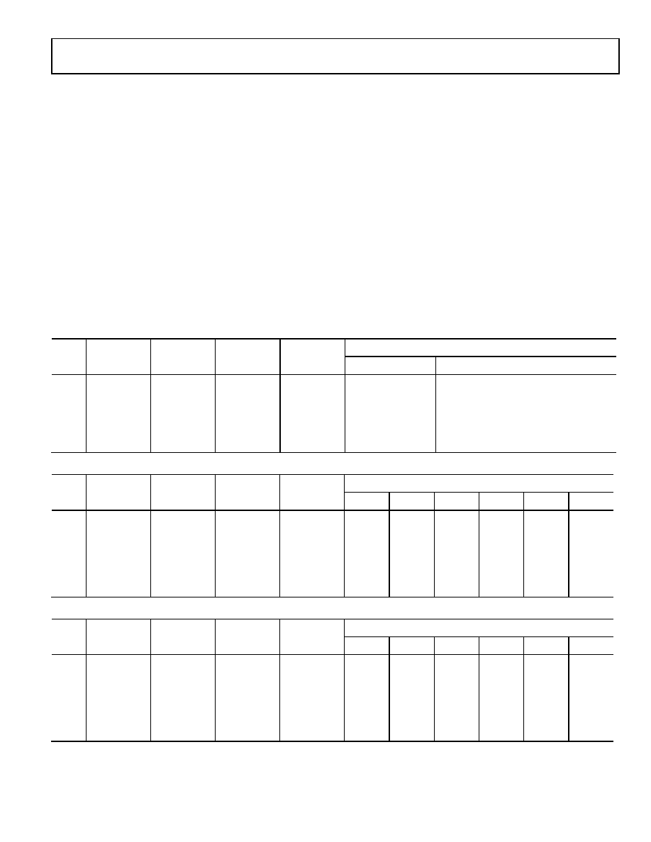
Table 5. Typical Output RMS Noise in V vs. Conversion Time and Input Range with Chopping Enabled
FW
Conversion
Time
Register
Conversion
Time (s)
Output Data
Rate (Hz)
3 dB
Frequency
(Hz)
Input Range/RMS Noise (V)
±2.5 V, +2.5 V
±1.25 V, +1.25 V, ±0.625 V, +0.625 V
127
0xFF
2689
372
200
1.8
1.1
46
0xAE
1001
999
500
2.7
1.7
17
0x91
397
2519
1325
4.8
2.7
10
0x8A
251
3982
2209
9.3
4.7
9
0x89
230
4342
2450
10.8
6.3
2
0x82
84
11838
9500
600
460
Table 6. Typical Effective Resolution in Bits vs. Conversion Time and Input Range with Chopping Enabled
FW
Conversion
Time
Register
Conversion
Time (s)
Output Data
Rate (Hz)
3 dB
Frequency
(Hz)
Input Range/Effective Resolution (Bits)
±2.5 V
+2.5 V
±1.25 V
+1.25 V ±0.625 V +0.625 V
127
0xFF
2689
372
200
21.4
20.4
21.2
20.2
19.2
46
0xAE
1001
999
500
20.8
19.8
20.5
19.5
18.5
17
0x91
397
2519
1325
20.0
19.0
19.8
18.8
17.8
10
0x8A
251
3982
2209
19.0
18.0
19.0
18.0
17.0
9
0x89
230
4342
2450
18.8
17.8
18.6
17.6
16.6
2
0x82
84
11838
9500
12.9
11.9
12.4
11.4
10.4
Table 7. Typical Peak-to-Peak Resolution in Bits vs. Conversion Time and Input Range with Chopping Enabled
FW
Conversion
Time
Register
Conversion
Time (s)
Output Data
Rate (Hz)
–3 dB
Frequency
(Hz)
Input Range/Peak-to-Peak Resolution (Bits)
±2.5 V
+2.5 V
±1.25 V
+1.25 V ±0.625 V +0.625 V
127
0xFF
2689
372
200
18.6
17.6
18.3
17.3
16.3
46
0xAE
1001
999
500
17.9
16.9
17.6
16.6
15.6
17
0x91
397
2519
1325
17.1
16.1
16.9
15.9
14.9
10
0x8A
251
3982
2209
16.2
15.2
16.2
15.2
14.2
9
0x89
230
4342
2450
16.0
15.0
15.8
14.8
13.8
2
0x82
84
11838
9500
10.7
0.7
9.7
8.7
7.7
相关PDF资料 |
PDF描述 |
|---|---|
| AD9223ARSZ-REEL | IC ADC 12BIT 3.0MSPS 28SSOP |
| AD9221ARSZ-REEL | IC ADC 12BIT 1.5MSPS 28SSOP |
| MS3106E22-22P | CONN PLUG 4POS STRAIGHT W/PINS |
| LTC1418IG#TRPBF | IC A/D CONV 14BIT SRL&PAR 28SSOP |
| D38999/20WD5PA | CONN RCPT 5POS WALL MNT W/PINS |
相关代理商/技术参数 |
参数描述 |
|---|---|
| AD773A | 制造商:AD 制造商全称:Analog Devices 功能描述:10-Bit, 20 MSPS Monolithic A/D Converter |
| AD773AJD | 制造商:Analog Devices 功能描述:ADC Single Pipelined 20Msps 10-bit Parallel 28-Pin CDIP 制造商:Rochester Electronics LLC 功能描述:IC, 10-BIT 20 MSPS ADC - Bulk |
| AD773AKD | 制造商:AD 制造商全称:Analog Devices 功能描述:10-Bit, 20 MSPS Monolithic A/D Converter |
| AD773ASD/883B | 制造商:未知厂家 制造商全称:未知厂家 功能描述:Analog-to-Digital Converter, 10-Bit |
| AD773-EB | 制造商:Rochester Electronics LLC 功能描述:- Bulk |
发布紧急采购,3分钟左右您将得到回复。