- 您现在的位置:买卖IC网 > PDF目录10212 > AD7853LARS (Analog Devices Inc)IC ADC 12BIT SRL 200KSPS 24-SSOP PDF资料下载
参数资料
| 型号: | AD7853LARS |
| 厂商: | Analog Devices Inc |
| 文件页数: | 24/34页 |
| 文件大小: | 0K |
| 描述: | IC ADC 12BIT SRL 200KSPS 24-SSOP |
| 标准包装: | 59 |
| 位数: | 12 |
| 采样率(每秒): | 100k |
| 数据接口: | 8051,QSPI?,串行,SPI? µP |
| 转换器数目: | 2 |
| 功率耗散(最大): | 33mW |
| 电压电源: | 模拟和数字 |
| 工作温度: | -40°C ~ 85°C |
| 安装类型: | 表面贴装 |
| 封装/外壳: | 24-SSOP(0.209",5.30mm 宽) |
| 供应商设备封装: | 24-SSOP |
| 包装: | 管件 |
| 输入数目和类型: | 1 个伪差分,单极;1 个伪差分,双极 |
第1页第2页第3页第4页第5页第6页第7页第8页第9页第10页第11页第12页第13页第14页第15页第16页第17页第18页第19页第20页第21页第22页第23页当前第24页第25页第26页第27页第28页第29页第30页第31页第32页第33页第34页
REV. B
–30–
AD7853/AD7853L
MICROPROCESSOR INTERFACING
In many applications, the user may not require the facility of
writing to the on-chip registers. The user may just want to
hardwire the relevant pins to the appropriate levels and read the
conversion result. In this case the DIN pin can be tied low so
that the on-chip registers are never used. Now the part will
operate as a nonprogrammable analog to digital converter where
the
CONVST is applied, a conversion is performed and the
result may be read using the SCLK to clock out the data from
the output register on to the DOUT pin. Note that the DIN pin
cannot be tied low when using the two-wire interface mode of
operation.
The SCLK can also be connected to the CLKIN pin if the user
does not want to have to provide separate serial and master
clocks in Interface Modes 1, 2, and 3. With this arrangement
the
SYNC signal must be low for 16 SCLK cycles in Interface
Modes 1 and 2 for the read and write operations. For Interface
Mode 3 the
SYNC can be low for more than 16 SCLK cycles
for the read and write operations. Note that in Interface Modes
4 and 5 the CLKIN and SCLK cannot be tied together as the
SCLK is an output and the CLKIN is an input.
DIN
DOUT
SYNC
CONVST
CLKIN
SCLK
AD7853/AD7853L
4 MHz/1.8MHz
MASTER
CLOCK
SYNC SIGNAL
TO GATE
THE SCLK
SERIAL DATA
OUTPUT
CONVERSION
START
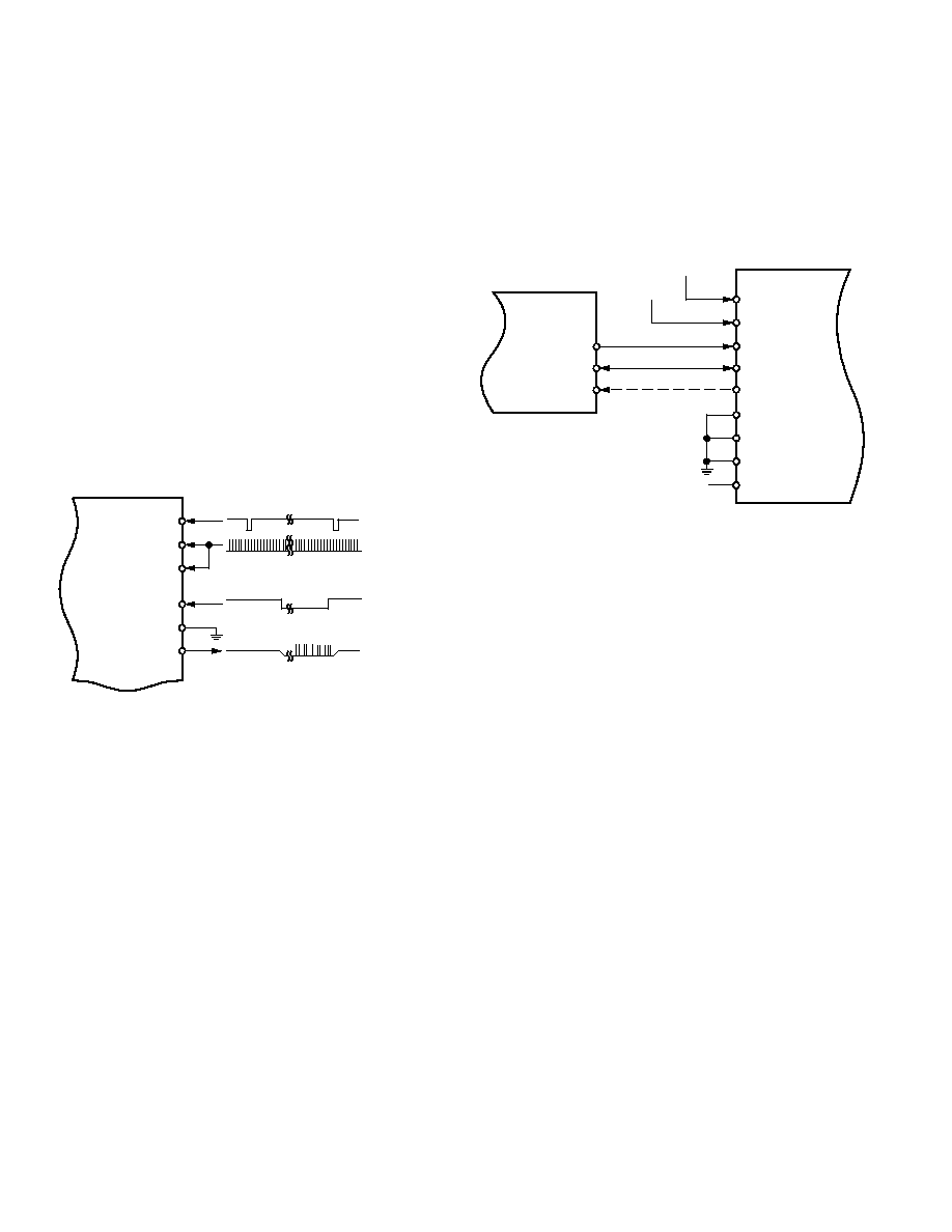
Figure 44. Simplified Interface Diagram with DIN
Grounded and SCLK Tied to CLKIN
AD7853/AD7853L to 8XC51/PIC17C42 Interface
Figure 45 shows the AD7853/AD7853L interface to the 8XC51/
PIC17C42. The 8XL51 is for interfacing to the AD7853/AD7853L
when the supply is at 3 V. The 8XC51/PIC17C42 only run at
5 V. The 8XC51 is in Mode 0 operation. This is a two-wire
interface consisting of the SCLK and the DIN which acts as a
bidirectional line. The
SYNC is tied low. The BUSY line can be
used to give an interrupt driven system but this would not nor-
mally be the case with the 8XC51/PIC17C42. For the 8XC51
12 MHz version, the serial clock will run at a maximum of
1 MHz so that the serial interface to the AD7853/AD7853L will
only be running at 1 MHz. The CLKIN signal must be provided
separately to the AD7853/AD7853L from a port line on the
8XC51 or from a source other than the 8XC51. Here the SCLK
cannot be tied to the CLKIN as the 8XC51 only provides a
noncontinuous serial clock. The
CONVST signal can be pro-
vided from an external timer or conversion can be started in
software if required. The sequence of events would typically be
writing to the control register via the DIN line setting a conver-
sion start and the 2-wire interface mode (this would be per-
formed in two 8-bit writes), wait for the conversion to be
finished (4.5
s with 4 MHz CLKIN), read the conversion re-
sult data on the DIN line (this would be performed in two 8-bit
reads), and then repeat the sequence. The maximum serial
frequency will be determined by the data access and hold times
of the 8XC51/PIC16C42 and the AD7853/AD7853L.
(8XC51/L51)
/PIC17C42
P3.0/DT
P3.1/CK
AD7853/AD7853L
CONVST
CLKIN
SCLK
DIN
SYNC
SM1
SM2
POLARITY
OPTIONAL
4MHz/1.8MHz
BUSY
(
INT0/P3.2)/INT
DVDD FOR 8XC51/L51
DGND FOR PIC17C42
MASTER
SLAVE
OPTIONAL
Figure 45. 8XC51/PIC17C42 Interface
AD7853/AD7853L to 68HC11/16/L11/PIC16C42 Interface
Figure 46 shows the AD7853/AD7853L SPI/QSPI interface to
the 68HC11/16/L11/PIC16C42. The 68L11 is for interfacing to
the AD7853/AD7853L when the supply is at 3 V. The
SYNC
line is not used and is tied to DGND. The
Controller is config-
ured as the master, by setting the MSTR bit in the SPCR to 1,
and thus provides the serial clock on the SCK pin. For all the
Controllers, the CPOL bit is set to 1 and for the 68HC11/16/
L11, the CPHA bit is set to 1. The CLKIN and
CONVST
signals can be supplied from the
Controller or from separate
sources. The BUSY signal can be used as an interrupt to tell the
Controller when the conversion is finished, then the reading
and writing can take place. If required the reading and writing
can take place during conversion and there will be no need for
the BUSY signal in this case. For no writing to the part then the
DIN pin can be tied permanently low. For the 68HC16 and the
QSPI interface the SM2 pin should be tied high and the
SS line
tied to the
SYNC pin. The microsequencer on the 68HC16
QSPI port can be used for performing a number of read and
write operations independent of the CPU and storing the con-
version results in memory without taxing the CPU. The typical
sequence of events would be writing to the control register via
the DIN line setting a conversion start and at the same time
reading data from the previous conversion on the DOUT line,
wait for the conversion to be finished (4.5
s with 4 MHz
CLKIN), and then repeat the sequence. The maximum serial
frequency will be determined by the data access and hold times
of the
Controllers and the AD7853/AD7853L.
相关PDF资料 |
PDF描述 |
|---|---|
| GTC030-16S-1P | CONN RCPT 7POS PANEL MNT W/PINS |
| AD7719BR-REEL7 | IC ADC 16BIT 24BIT DUAL 28-SOIC |
| MS27484T12F3SD | CONN PLUG 3POS STRAIGHT W/SCKT |
| SP3088EEN-L/TR | IC TXRX RS485/RS422 ESD 8NSOIC |
| AD7951BCPZRL | IC ADC 14BIT 1MSPS 48-LFCSP |
相关代理商/技术参数 |
参数描述 |
|---|---|
| AD7853LARS-REEL | 功能描述:IC ADC 12BIT SRL 200KSPS 24-SSOP RoHS:否 类别:集成电路 (IC) >> 数据采集 - 模数转换器 系列:- 标准包装:1,000 系列:- 位数:12 采样率(每秒):300k 数据接口:并联 转换器数目:1 功率耗散(最大):75mW 电压电源:单电源 工作温度:0°C ~ 70°C 安装类型:表面贴装 封装/外壳:24-SOIC(0.295",7.50mm 宽) 供应商设备封装:24-SOIC 包装:带卷 (TR) 输入数目和类型:1 个单端,单极;1 个单端,双极 |
| AD7853LARSZ | 功能描述:IC ADC 12BIT SRL 200KSPS 24SSOP RoHS:是 类别:集成电路 (IC) >> 数据采集 - 模数转换器 系列:- 标准包装:1,000 系列:- 位数:12 采样率(每秒):300k 数据接口:并联 转换器数目:1 功率耗散(最大):75mW 电压电源:单电源 工作温度:0°C ~ 70°C 安装类型:表面贴装 封装/外壳:24-SOIC(0.295",7.50mm 宽) 供应商设备封装:24-SOIC 包装:带卷 (TR) 输入数目和类型:1 个单端,单极;1 个单端,双极 |
| AD7853LARSZ-REEL | 功能描述:IC ADC 12BIT SRL 200KSPS 24SSOP RoHS:是 类别:集成电路 (IC) >> 数据采集 - 模数转换器 系列:- 标准包装:1,000 系列:- 位数:16 采样率(每秒):45k 数据接口:串行 转换器数目:2 功率耗散(最大):315mW 电压电源:模拟和数字 工作温度:0°C ~ 70°C 安装类型:表面贴装 封装/外壳:28-SOIC(0.295",7.50mm 宽) 供应商设备封装:28-SOIC W 包装:带卷 (TR) 输入数目和类型:2 个单端,单极 |
| AD7853LARZ | 功能描述:IC ADC 12BIT SRL 200KSPS 24SOIC RoHS:是 类别:集成电路 (IC) >> 数据采集 - 模数转换器 系列:- 标准包装:1,000 系列:- 位数:12 采样率(每秒):300k 数据接口:并联 转换器数目:1 功率耗散(最大):75mW 电压电源:单电源 工作温度:0°C ~ 70°C 安装类型:表面贴装 封装/外壳:24-SOIC(0.295",7.50mm 宽) 供应商设备封装:24-SOIC 包装:带卷 (TR) 输入数目和类型:1 个单端,单极;1 个单端,双极 |
| AD7853LARZ-REEL | 功能描述:IC ADC 12BIT SRL 200KSPS 24SOIC RoHS:是 类别:集成电路 (IC) >> 数据采集 - 模数转换器 系列:- 产品培训模块:Lead (SnPb) Finish for COTS Obsolescence Mitigation Program 标准包装:2,500 系列:- 位数:12 采样率(每秒):3M 数据接口:- 转换器数目:- 功率耗散(最大):- 电压电源:- 工作温度:- 安装类型:表面贴装 封装/外壳:SOT-23-6 供应商设备封装:SOT-23-6 包装:带卷 (TR) 输入数目和类型:- |
发布紧急采购,3分钟左右您将得到回复。