- 您现在的位置:买卖IC网 > PDF目录10212 > AD7853LARS (Analog Devices Inc)IC ADC 12BIT SRL 200KSPS 24-SSOP PDF资料下载
参数资料
| 型号: | AD7853LARS |
| 厂商: | Analog Devices Inc |
| 文件页数: | 32/34页 |
| 文件大小: | 0K |
| 描述: | IC ADC 12BIT SRL 200KSPS 24-SSOP |
| 标准包装: | 59 |
| 位数: | 12 |
| 采样率(每秒): | 100k |
| 数据接口: | 8051,QSPI?,串行,SPI? µP |
| 转换器数目: | 2 |
| 功率耗散(最大): | 33mW |
| 电压电源: | 模拟和数字 |
| 工作温度: | -40°C ~ 85°C |
| 安装类型: | 表面贴装 |
| 封装/外壳: | 24-SSOP(0.209",5.30mm 宽) |
| 供应商设备封装: | 24-SSOP |
| 包装: | 管件 |
| 输入数目和类型: | 1 个伪差分,单极;1 个伪差分,双极 |
第1页第2页第3页第4页第5页第6页第7页第8页第9页第10页第11页第12页第13页第14页第15页第16页第17页第18页第19页第20页第21页第22页第23页第24页第25页第26页第27页第28页第29页第30页第31页当前第32页第33页第34页
REV. B
–7–
AD7853/AD7853L
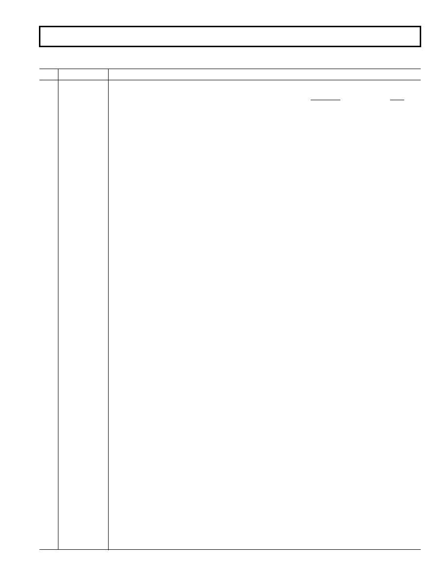
PIN FUNCTION DESCRIPTIONS
Pin
Mnemonic
Description
1
CONVST
Convert Start. Logic Input. A low to high transition on this input puts the track/hold into its hold mode and
starts conversion. When this input is not used, it should be tied to DVDD.
2
BUSY
Busy Output. The busy output is triggered high by the falling edge of
CONVST or rising edge of CAL, and
remains high until conversion is completed. BUSY is also used to indicate when the AD7853/AD7853L has
completed its on-chip calibration sequence.
3
SLEEP
Sleep Input/Low Power Mode. A Logic 0 initiates a sleep and all circuitry is powered down including the
internal voltage reference provided there is no conversion or calibration being performed. Calibration data
is retained. A Logic 1 results in normal operation. See Power-Down section for more details.
4
REFIN/
Reference Input/Output. This pin is connected to the internal reference through a series resistor and is the
REFOUT
reference source for the analog-to-digital converter. The nominal reference voltage is 2.5 V and this appears
at the pin. This pin can be overdriven by an external reference or can be taken as high as AVDD. When this
pin is tied to AVDD, or when an externally applied reference approaches AVDD, the CREF1 pin should also be
tied to AVDD.
5AVDD
Analog Positive Supply Voltage, +3.0 V to +5.5 V.
6, 12 AGND
Analog Ground. Ground reference for track/hold, reference and DAC.
7CREF1
Reference Capacitor (0.1
F multilayer ceramic). This external capacitor is used as a charge source for the
internal DAC. The capacitor should be tied between the pin and AGND.
8CREF2
Reference Capacitor (0.01
F ceramic disc). This external capacitor is used in conjunction with the on-chip
reference. The capacitor should be tied between the pin and AGND.
9
AIN(+)
Analog Input. Positive input of the pseudo-differential analog input. Cannot go below AGND or above
AVDD at any time, and cannot go below AIN(–) when the unipolar input range is selected.
10
AIN(–)
Analog Input. Negative input of the pseudo-differential analog input. Cannot go below AGND or above
AVDD at any time.
11
NC
No Connect Pin.
13
AMODE
Analog Mode Pin. This pin allows two different analog input ranges to be selected. A Logic 0 selects range
0 to VREF (i.e., AIN(+) – AIN(–) = 0 to VREF). In this case AIN(+) cannot go below AIN(–) and
AIN(–) cannot go below AGND. A Logic 1 selects range –VREF/2 to +VREF/2 (i.e., AIN(+) – AIN(–) =
–VREF/2 to +VREF/2). In this case AIN(+) cannot go below AGND so that AIN(–) needs to be biased to
+VREF/2 to allow AIN(+) to go from 0 V to +VREF V.
14
POLARITY
Serial Clock Polarity. This pin determines the active edge of the serial clock (SCLK). Toggling this pin will
reverse the active edge of the serial clock (SCLK). A Logic 1 means that the serial clock (SCLK) idles high
and a Logic 0 means that the serial clock (SCLK) idles low. It is best to refer to the timing diagrams and
Table IX for the SCLK active edges.
15
SM1
Serial Mode Select Pin. This pin is used in conjunction with the SM2 pin to give different modes of opera-
tion as described in Table X.
16
SM2
Serial Mode Select Pin. This pin is used in conjunction with the SM1 pin to give different modes of opera-
tion as described in Table X.
17
CAL
Calibration Input. This pin has an internal pull-up current source of 0.15
A. A Logic 0 on this pin resets
all calibration control logic and initiates a calibration on its rising edge. There is the option of connecting a
10 nF capacitor from this pin to DGND to allow for an automatic self-calibration on power-up. This input
overrides all other internal operations. If the autocalibration is not required, this pin should be tied to a
logic high.
18
DVDD
Digital Supply Voltage, +3.0 V to +5.5 V.
19
DGND
Digital Ground. Ground reference point for digital circuitry.
20
DOUT
Serial Data Output. The data output is supplied to this pin as a 16-bit serial word.
21
DIN
Serial Data Input. The data to be written is applied to this pin in serial form (16-bit word). This pin can act
as an input pin or as a I/O pin depending on the serial interface mode the part is in (see Table X).
22
CLKIN
Master Clock Signal for the device (4 MHz for AD7853, 1.8 MHz for AD7853L). Sets the conversion and
calibration times.
23
SCLK
Serial Port Clock. Logic input/output. The SCLK pin is configured as an input or output, dependent on the
type of serial data transmission (self-clocking or external-clocking) that has been selected by the SM1 and
SM2 pins. The SCLK idles high or low depending on the state of the POLARITY pin.
24
SYNC
This pin can be an input level triggered active low (similar to a chip select in one case and to a frame sync
in the other) or an output (similar to a frame sync) pin depending on SM1, SM2 (see Table X).
相关PDF资料 |
PDF描述 |
|---|---|
| GTC030-16S-1P | CONN RCPT 7POS PANEL MNT W/PINS |
| AD7719BR-REEL7 | IC ADC 16BIT 24BIT DUAL 28-SOIC |
| MS27484T12F3SD | CONN PLUG 3POS STRAIGHT W/SCKT |
| SP3088EEN-L/TR | IC TXRX RS485/RS422 ESD 8NSOIC |
| AD7951BCPZRL | IC ADC 14BIT 1MSPS 48-LFCSP |
相关代理商/技术参数 |
参数描述 |
|---|---|
| AD7853LARS-REEL | 功能描述:IC ADC 12BIT SRL 200KSPS 24-SSOP RoHS:否 类别:集成电路 (IC) >> 数据采集 - 模数转换器 系列:- 标准包装:1,000 系列:- 位数:12 采样率(每秒):300k 数据接口:并联 转换器数目:1 功率耗散(最大):75mW 电压电源:单电源 工作温度:0°C ~ 70°C 安装类型:表面贴装 封装/外壳:24-SOIC(0.295",7.50mm 宽) 供应商设备封装:24-SOIC 包装:带卷 (TR) 输入数目和类型:1 个单端,单极;1 个单端,双极 |
| AD7853LARSZ | 功能描述:IC ADC 12BIT SRL 200KSPS 24SSOP RoHS:是 类别:集成电路 (IC) >> 数据采集 - 模数转换器 系列:- 标准包装:1,000 系列:- 位数:12 采样率(每秒):300k 数据接口:并联 转换器数目:1 功率耗散(最大):75mW 电压电源:单电源 工作温度:0°C ~ 70°C 安装类型:表面贴装 封装/外壳:24-SOIC(0.295",7.50mm 宽) 供应商设备封装:24-SOIC 包装:带卷 (TR) 输入数目和类型:1 个单端,单极;1 个单端,双极 |
| AD7853LARSZ-REEL | 功能描述:IC ADC 12BIT SRL 200KSPS 24SSOP RoHS:是 类别:集成电路 (IC) >> 数据采集 - 模数转换器 系列:- 标准包装:1,000 系列:- 位数:16 采样率(每秒):45k 数据接口:串行 转换器数目:2 功率耗散(最大):315mW 电压电源:模拟和数字 工作温度:0°C ~ 70°C 安装类型:表面贴装 封装/外壳:28-SOIC(0.295",7.50mm 宽) 供应商设备封装:28-SOIC W 包装:带卷 (TR) 输入数目和类型:2 个单端,单极 |
| AD7853LARZ | 功能描述:IC ADC 12BIT SRL 200KSPS 24SOIC RoHS:是 类别:集成电路 (IC) >> 数据采集 - 模数转换器 系列:- 标准包装:1,000 系列:- 位数:12 采样率(每秒):300k 数据接口:并联 转换器数目:1 功率耗散(最大):75mW 电压电源:单电源 工作温度:0°C ~ 70°C 安装类型:表面贴装 封装/外壳:24-SOIC(0.295",7.50mm 宽) 供应商设备封装:24-SOIC 包装:带卷 (TR) 输入数目和类型:1 个单端,单极;1 个单端,双极 |
| AD7853LARZ-REEL | 功能描述:IC ADC 12BIT SRL 200KSPS 24SOIC RoHS:是 类别:集成电路 (IC) >> 数据采集 - 模数转换器 系列:- 产品培训模块:Lead (SnPb) Finish for COTS Obsolescence Mitigation Program 标准包装:2,500 系列:- 位数:12 采样率(每秒):3M 数据接口:- 转换器数目:- 功率耗散(最大):- 电压电源:- 工作温度:- 安装类型:表面贴装 封装/外壳:SOT-23-6 供应商设备封装:SOT-23-6 包装:带卷 (TR) 输入数目和类型:- |
发布紧急采购,3分钟左右您将得到回复。