- 您现在的位置:买卖IC网 > PDF目录10218 > AD7856ARSZ-REEL7 (Analog Devices Inc)IC ADC 14BIT 8CHAN 5V 24SSOP PDF资料下载
参数资料
| 型号: | AD7856ARSZ-REEL7 |
| 厂商: | Analog Devices Inc |
| 文件页数: | 16/32页 |
| 文件大小: | 0K |
| 描述: | IC ADC 14BIT 8CHAN 5V 24SSOP |
| 标准包装: | 500 |
| 位数: | 14 |
| 采样率(每秒): | 285k |
| 数据接口: | 8051,QSPI?,串行,SPI? µP |
| 转换器数目: | 2 |
| 功率耗散(最大): | 89.25mW |
| 电压电源: | 模拟和数字 |
| 工作温度: | -40°C ~ 105°C |
| 安装类型: | 表面贴装 |
| 封装/外壳: | 24-SSOP(0.209",5.30mm 宽) |
| 供应商设备封装: | 24-SSOP |
| 包装: | 带卷 (TR) |
| 输入数目和类型: | 8 个单端,单极;4 个伪差分,单极 |
第1页第2页第3页第4页第5页第6页第7页第8页第9页第10页第11页第12页第13页第14页第15页当前第16页第17页第18页第19页第20页第21页第22页第23页第24页第25页第26页第27页第28页第29页第30页第31页第32页
AD7856
–23–
REV. A
required to reduced the offset and gain errors to at least the 14-
bit level. There will never be any need to perform more than
three system (offset + gain) calibrations.
The zero scale error is adjusted for an offset calibration and the
positive full-scale error is adjusted for a gain calibration.
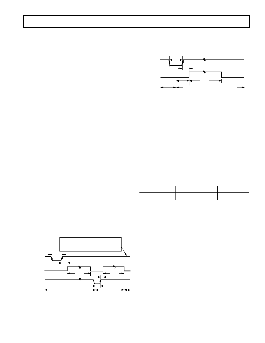
System Calibration Timing
The calibration timing diagram in Figure 29 is for a full system
calibration where the falling edge of
CAL initiates an internal
reset before starting a calibration (note that if the part is in power-
down mode, the
CAL pulsewidth must take account of the power-up
time). For software calibrations with power-down modes, see
note in Power-Up Times section. If a full system calibration is
to be performed in software it is easier to perform separate gain
and offset calibrations so that the CONVST bit in the control
register does not have to be programmed in the middle of the
system calibration sequence. The rising edge of
CAL starts
calibration of the internal DAC and causes the BUSY line to go
high. If the control register is set for a full system calibration,
the
CONVST must be used also. The full-scale system voltage
should be applied to the analog input pins from the start of
calibration. The BUSY line will go low once the DAC and Sys-
tem Gain Calibration are complete. Next the system offset volt-
age is applied to the AIN pin for a minimum setup time (tSETUP)
of 100 ns before the rising edge of the
CONVST and remains
until the BUSY signal goes low. The rising edge of the
CONVST
starts the system offset calibration section of the full system
calibration and also causes the BUSY signal to go high. The
BUSY signal will go low after a time tCAL2 when the calibration
sequence is complete. In some applications not all the input
channels may be used. In this case it may be useful to dedicate
two input channels for the system calibration, one which has the
system offset voltage applied to it, and one which has the system
full scale voltage applied to it. When a system offset or gain
calibration is performed, the channel selected should correspond
to the system offset or system full-scale voltage channel.
The timing for a system (gain + offset) calibration is very similar
to that of Figure 29 the only difference being that the time tCAL1
will be replaced by a shorter time of the order of tCAL2 as the
internal DAC will not be calibrated. The BUSY signal will
signify when the gain calibration is finished and when the part is
ready for the offset calibration.
CONVST (I/P)
AIN (I/P)
t16
tSETUP
CAL (I/P)
BUSY (O/P)
t1
t15
t1 = 100ns MIN, t16 = 2.5 tCLKIN MAX,
t15 = 2.5 tCLKIN MAX, tCAL1 = 222228 tCLKIN MAX,
tCAL2 = 27798 tCLKIN
tCAL1
tCAL2
VSYSTEM FULL SCALE
VOFFSET
Figure 29. Timing Diagram for Full System Calibration
The timing diagram for a system offset or system gain calibra-
tion is shown in Figure 30. Here again the
CAL is pulsed and
the rising edge of the
CAL initiates the calibration sequence (or
the calibration can be initiated in software by writing to the
control register). The rising edge of the
CAL causes the BUSY
line to go high and it will stay high until the calibration sequence is
finished. The analog input should be set at the correct level for a
minimum setup time (tSETUP) of 100 ns before the rising edge of
CAL and stay at the correct level until the BUSY signal goes low.
AIN (I/P)
t
SETUP
BUSY (O/P)
t15
t1
VSYSTEM FULL SCALE OR VSYSTEM OFFSET
CAL (I/P)
tCAL2
Figure 30. Timing Diagram for System Gain or System
Offset Calibration
SERIAL INTERFACE SUMMARY
Table IX details the two interface modes and the serial clock
edges from which the data is clocked out by the AD7856
(DOUT Edge) and that the data is latched in on (DIN Edge).
In both interface Modes 1, and 2 the
SYNC is gated with the
SCLK. Thus the falling edge of
SYNC may clock out the MSB
of data. Subsequent bits will be clocked out by the Serial Clock,
SCLK. The condition for the falling edge of
SYNC clocking out
the MSB of data is as follows:
The falling edge of
SYNC will clock out the MSB if the serial clock
is low when the
SYNC goes low.
If this condition is not the case, the SCLK will clock out the
MSB. If a noncontinuous SCLK is used, it should idle high.
Table IX. SCLK Active Edges
Interface Mode
DOUT Edge
DIN Edge
1, 2
SCLK
↓
SCLK
↑
Resetting the Serial Interface
When writing to the part via the DIN line there is the possibility
of writing data into the incorrect registers, such as the test regis-
ter for instance, or writing the incorrect data and corrupting the
serial interface. The
SYNC pin acts as a reset. Bringing the
SYNC pin high resets the internal shift register. The first data
bit after the next
SYNC falling edge will now be the first bit of a
new 16-bit transfer. It is also possible that the test register con-
tents were altered when the interface was lost. Therefore, once
the serial interface is reset it may be necessary to write the 16-bit
word 0100 0000 0000 0010 to restore the test register to its
default value. Now the part and serial interface are completely
reset. It is always useful to retain the ability to program the
SYNC line from a port of the
Controller/DSP to have the abil-
ity to reset the serial interface.
Table X summarizes the interface modes provided by the
AD7856. It also outlines the various
P/C to which the par-
ticular interface is suited.
Interface Mode 1 may only be set by programming the control
register (See section on Control Register).
Some of the more popular
Processors, Controllers, and DSP
machines that the AD7856 will interface to directly are men-
tioned here. This does not cover all
Cs, Ps and DSPs. A more
detailed timing description on each of the interface modes follows.
相关PDF资料 |
PDF描述 |
|---|---|
| VI-21J-IU-F3 | CONVERTER MOD DC/DC 36V 200W |
| CS8416-CNZ | IC RCVR DGTL 192KHZ 28QFN COMM |
| VI-21J-IU-F2 | CONVERTER MOD DC/DC 36V 200W |
| SP3494EN-L/TR | IC TXRX RS485/RS422 LP 8NSOIC |
| SP3491EN-L/TR | IC TXRX RS485 FULL DUPLX 14NSOIC |
相关代理商/技术参数 |
参数描述 |
|---|---|
| AD7856ARZ | 功能描述:IC ADC 14BIT 8CHAN 5V 24SOIC RoHS:是 类别:集成电路 (IC) >> 数据采集 - 模数转换器 系列:- 其它有关文件:TSA1204 View All Specifications 标准包装:1 系列:- 位数:12 采样率(每秒):20M 数据接口:并联 转换器数目:2 功率耗散(最大):155mW 电压电源:模拟和数字 工作温度:-40°C ~ 85°C 安装类型:表面贴装 封装/外壳:48-TQFP 供应商设备封装:48-TQFP(7x7) 包装:Digi-Reel® 输入数目和类型:4 个单端,单极;2 个差分,单极 产品目录页面:1156 (CN2011-ZH PDF) 其它名称:497-5435-6 |
| AD7856ARZ-REEL7 | 功能描述:IC ADC 14BIT 8CHAN 5V 24SOIC RoHS:是 类别:集成电路 (IC) >> 数据采集 - 模数转换器 系列:- 产品培训模块:Lead (SnPb) Finish for COTS Obsolescence Mitigation Program 标准包装:2,500 系列:- 位数:12 采样率(每秒):3M 数据接口:- 转换器数目:- 功率耗散(最大):- 电压电源:- 工作温度:- 安装类型:表面贴装 封装/外壳:SOT-23-6 供应商设备封装:SOT-23-6 包装:带卷 (TR) 输入数目和类型:- |
| AD7856KR | 制造商:Analog Devices 功能描述:ADC Single SAR 285ksps 14-bit Serial 24-Pin SOIC W 制造商:Rochester Electronics LLC 功能描述:8 CH. 14-BIT 300 KSPS ADC I.C. - Bulk |
| AD7856KR-REEL | 功能描述:IC ADC 14BIT 8CH 5V 24-SOIC RoHS:否 类别:集成电路 (IC) >> 数据采集 - 模数转换器 系列:- 标准包装:1,000 系列:- 位数:12 采样率(每秒):300k 数据接口:并联 转换器数目:1 功率耗散(最大):75mW 电压电源:单电源 工作温度:0°C ~ 70°C 安装类型:表面贴装 封装/外壳:24-SOIC(0.295",7.50mm 宽) 供应商设备封装:24-SOIC 包装:带卷 (TR) 输入数目和类型:1 个单端,单极;1 个单端,双极 |
| AD7856KR-REEL7 | 制造商:Analog Devices 功能描述:ADC Single SAR 285ksps 14-bit Serial 24-Pin SOIC W T/R 制造商:Rochester Electronics LLC 功能描述:8 CH. 14-BIT 300 KSPS ADC I.C. - Tape and Reel |
发布紧急采购,3分钟左右您将得到回复。