- 您现在的位置:买卖IC网 > PDF目录10160 > AD7856KRZ (Analog Devices Inc)IC ADC 14BIT 8CHAN 5V 24SOIC PDF资料下载
参数资料
| 型号: | AD7856KRZ |
| 厂商: | Analog Devices Inc |
| 文件页数: | 15/32页 |
| 文件大小: | 0K |
| 描述: | IC ADC 14BIT 8CHAN 5V 24SOIC |
| 标准包装: | 31 |
| 位数: | 14 |
| 采样率(每秒): | 285k |
| 数据接口: | 8051,QSPI?,串行,SPI? µP |
| 转换器数目: | 2 |
| 功率耗散(最大): | 89.25mW |
| 电压电源: | 模拟和数字 |
| 工作温度: | 0°C ~ 105°C |
| 安装类型: | 表面贴装 |
| 封装/外壳: | 24-SOIC(0.295",7.50mm 宽) |
| 供应商设备封装: | 24-SOIC W |
| 包装: | 管件 |
| 输入数目和类型: | 8 个单端,单极;4 个伪差分,单极 |
第1页第2页第3页第4页第5页第6页第7页第8页第9页第10页第11页第12页第13页第14页当前第15页第16页第17页第18页第19页第20页第21页第22页第23页第24页第25页第26页第27页第28页第29页第30页第31页第32页
AD7856
–22–
REV. A
is initiated. Typical figures are given in Table VIII. The timing
diagrams for the other self-calibration options will be similar to
that outlined in Figure 25.
t1 = 100ns MIN,
t15 = 2.5 tCLKIN MAX,
tCAL = 250026 tCLKIN
CAL (I/P)
BUSY (O/P)
t1
t15
tCAL
Figure 25. Timing Diagram for Full-Self Calibration
System Calibration Description
System calibration allows the user to take out system errors
external to the AD7856 as well as calibrate the errors of the
AD7856 itself. The maximum calibration range specified for the
system offset errors is
±3.75% of V
REF but typically is ± 5% and
for the system gain errors is
±1.875% of V
REF. Therefore, under
worst case conditions the maximum allowable system offset
voltage applied between AIN(+) and AIN(–) would be
±0.0375
× V
REF, but under typical conditions this means that the maxi-
mum allowable system offset voltage applied between the AIN(+)
and AIN(–) pins for the calibration to adjust out this error is
±0.05
× V
REF (i.e., the AIN(+) can be 0.05
× V
REF above AIN(–)
or 0.05
× V
REF below AIN(–)). For the System gain error the
maximum allowable system full-scale voltage that can be applied
between AIN(+) and AIN(–) for the calibration to adjust out
this error is VREF
± 0.01875
× V
REF (i.e., the AIN(+) can be VREF
+ 0.01875
× V
REF above AIN(–) or VREF – 0.01875 × VREF above
AIN(–)). If the system offset or system gain errors are outside
the ranges mentioned the system calibration algorithm will
reduce the errors as much as the trim range allows.
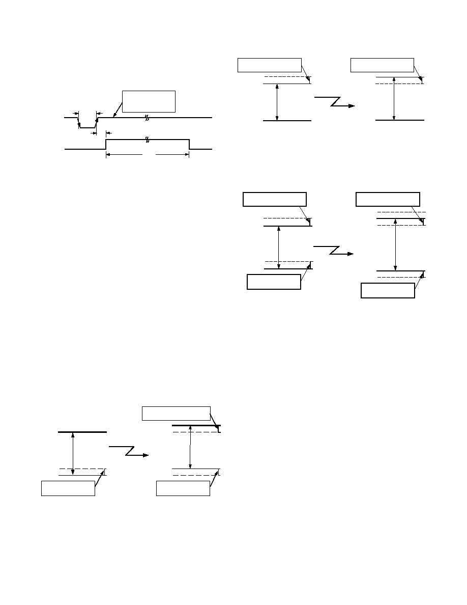
Figures 26 through 28 illustrate why a specific type of system
calibration might be used. Figure 26 shows a system offset cali-
bration (assuming a positive offset) where the analog input
range has been shifted upward by the system offset after the
system offset calibration is completed. A negative offset may
also be accounted for by a system offset calibration.
SYSTEM OFFSET
CALIBRATION
SYS OFFSET
VREF – 1LSB
AGND
MAX SYSTEM OFFSET
IS
5% OF VREF
MAX SYSTEM FULL SCALE
IS
1.875% FROM VREF
ANALOG
INPUT
RANGE
VREF – 1LSB
ANALOG
INPUT
RANGE
SYS OFFSET
AGND
MAX SYSTEM OFFSET
IS
5% OF VREF
VREF + SYS OFFSET
Figure 26. System Offset Calibration
Figure 27 shows a system gain calibration (assuming a system
full scale greater than the reference voltage) where the analog
input range has been increased after the system gain calibration
is completed. A system full-scale voltage less than the reference
voltage may also be accounted for by a system gain calibration.
SYSTEM GAIN
CALIBRATION
VREF – 1LSB
AGND
MAX SYSTEM FULL SCALE
IS
1.875% FROM VREF
ANALOG
INPUT
RANGE
VREF – 1LSB
ANALOG
INPUT
RANGE
AGND
SYS FS
MAX SYSTEM FULL SCALE
IS
1.875% FROM VREF
Figure 27. System Gain Calibration
Finally, in Figure 28 both the system offset and gain are ac-
counted for by the system offset followed by a system gain cali-
bration. First, the analog input range is shifted upward by the
positive system offset and then the analog input range is ad-
justed at the top end to account for the system full scale.
SYSTEM OFFSET
CALIBRATION
FOLLOWED BY
SYSTEM GAIN
CALIBRATION
SYS OFFSET
VREF – 1LSB
AGND
MAX SYSTEM OFFSET
IS
5% OF VREF
MAX SYSTEM FULL SCALE
IS
1.875% FROM VREF
ANALOG
INPUT
RANGE
VREF – 1LSB
ANALOG
INPUT
RANGE
SYS OFFSET
AGND
MAX SYSTEM OFFSET
IS
5% OF VREF
VREF + SYS OFFSET
SYS FS
MAX SYSTEM FULL SCALE
IS
1.875% FROM VREF
SYS FS
Figure 28. System (Gain + Offset) Calibration
System Gain and Offset Interaction
The inherent architecture of the AD7856 leads to an interaction
between the system offset and gain errors when a system calibra-
tion is performed. Therefore, it is recommended to perform the
cycle of a system offset calibration followed by a system gain
calibration twice. Separate system offset and system gain cali-
brations reduce the offset and gain errors to at least the 14-bit
level. By performing a system offset
CAL first and a system gain
calibration second, priority is given to reducing the gain error to
zero before reducing the offset error to zero. If the system errors
are small, a system offset calibration would be performed, fol-
lowed by a system gain calibration. If the systems errors are
large (close to the specified limits of the calibration range), this
cycle would be repeated twice to ensure that the offset and gain
errors were reduced to at least the 14-bit level. The advantage of
doing separate system offset and system gain calibrations is that
the user has more control over when the analog inputs need to
be at the required levels, and the
CONVST signal does not have
to be used.
Alternatively, a system (gain + offset) calibration can be
performed. It is recommended to perform three system (gain +
offset) calibrations to reduce the offset and gain errors to the 14-
bit level. For the system (gain + offset) calibration priority is
given to reducing the offset error to zero before reducing the
gain error to zero. Thus if the system errors are small then two
system (gain + offset) calibrations will be sufficient. If the sys-
tem errors are large (close to the specified limits of the calibra-
tion range) three system (gain + offset) calibrations may be
相关PDF资料 |
PDF描述 |
|---|---|
| LTC2392CLX-16#PBF | IC ADC 16BIT SER/PAR 500K 48LQFP |
| ADM3078EYRZ-REEL7 | TXRX 3V 15KV 500KBPS ESD 8-SOIC |
| AD7572AJRZ10 | IC ADC 12BIT HS LC2MOS 24SOIC |
| ADM211EARU-REEL | IC TXRX RS-232 5V 0.1UF 28TSSOP |
| ADM207EARU-REEL | IC TXRX RS232 5DVR/3REC 24TSSOP |
相关代理商/技术参数 |
参数描述 |
|---|---|
| AD7858 | 制造商:AD 制造商全称:Analog Devices 功能描述:3 V to 5 V Single Supply, 200 kSPS 8-Channel, 12-Bit Sampling ADC |
| AD7858AN | 功能描述:IC ADC 12BIT 8CH SRL 24-DIP RoHS:否 类别:集成电路 (IC) >> 数据采集 - 模数转换器 系列:- 标准包装:1 系列:- 位数:14 采样率(每秒):83k 数据接口:串行,并联 转换器数目:1 功率耗散(最大):95mW 电压电源:双 ± 工作温度:0°C ~ 70°C 安装类型:通孔 封装/外壳:28-DIP(0.600",15.24mm) 供应商设备封装:28-PDIP 包装:管件 输入数目和类型:1 个单端,双极 |
| AD7858ANZ | 功能描述:IC ADC 12BIT 8CHAN SRL 24-DIP RoHS:是 类别:集成电路 (IC) >> 数据采集 - 模数转换器 系列:- 标准包装:1,000 系列:- 位数:12 采样率(每秒):300k 数据接口:并联 转换器数目:1 功率耗散(最大):75mW 电压电源:单电源 工作温度:0°C ~ 70°C 安装类型:表面贴装 封装/外壳:24-SOIC(0.295",7.50mm 宽) 供应商设备封装:24-SOIC 包装:带卷 (TR) 输入数目和类型:1 个单端,单极;1 个单端,双极 |
| AD7858AR | 功能描述:IC ADC 12BIT 8CH SRL 24-SOIC RoHS:否 类别:集成电路 (IC) >> 数据采集 - 模数转换器 系列:- 标准包装:1,000 系列:- 位数:12 采样率(每秒):300k 数据接口:并联 转换器数目:1 功率耗散(最大):75mW 电压电源:单电源 工作温度:0°C ~ 70°C 安装类型:表面贴装 封装/外壳:24-SOIC(0.295",7.50mm 宽) 供应商设备封装:24-SOIC 包装:带卷 (TR) 输入数目和类型:1 个单端,单极;1 个单端,双极 |
| AD7858AR-REEL | 制造商:Analog Devices 功能描述:ADC Single SAR 200ksps 12-bit Serial 24-Pin SOIC W T/R 制造商:Analog Devices 功能描述:ADC SGL SAR 200KSPS 12-BIT SERL 24SOIC W - Tape and Reel 制造商:Rochester Electronics LLC 功能描述:SELF CAL.SERIAL 8CH. 12-BIT ADC I.C. - Tape and Reel |
发布紧急采购,3分钟左右您将得到回复。