- 您现在的位置:买卖IC网 > PDF目录10160 > AD7856KRZ (Analog Devices Inc)IC ADC 14BIT 8CHAN 5V 24SOIC PDF资料下载
参数资料
| 型号: | AD7856KRZ |
| 厂商: | Analog Devices Inc |
| 文件页数: | 17/32页 |
| 文件大小: | 0K |
| 描述: | IC ADC 14BIT 8CHAN 5V 24SOIC |
| 标准包装: | 31 |
| 位数: | 14 |
| 采样率(每秒): | 285k |
| 数据接口: | 8051,QSPI?,串行,SPI? µP |
| 转换器数目: | 2 |
| 功率耗散(最大): | 89.25mW |
| 电压电源: | 模拟和数字 |
| 工作温度: | 0°C ~ 105°C |
| 安装类型: | 表面贴装 |
| 封装/外壳: | 24-SOIC(0.295",7.50mm 宽) |
| 供应商设备封装: | 24-SOIC W |
| 包装: | 管件 |
| 输入数目和类型: | 8 个单端,单极;4 个伪差分,单极 |
第1页第2页第3页第4页第5页第6页第7页第8页第9页第10页第11页第12页第13页第14页第15页第16页当前第17页第18页第19页第20页第21页第22页第23页第24页第25页第26页第27页第28页第29页第30页第31页第32页
AD7856
–24–
REV. A
Table X. Interface Mode Description
Interface
Processor/
Mode
Controller
Comment
1
8XC51
(2-Wire)
8XL51
(DIN Is an Input/
PIC17C42
Output Pin)
2
68HC11
(3-Wire, SPI)
68L11
(Default Mode)
68HC16
PIC16C64
ADSP-21xx
DSP56000
DSP56001
DSP56002
DSP56L002
DETAILED TIMING SECTION
Mode 1 (2-Wire 8051 Interface)
The read and write takes place on the DIN line and the conver-
sion is initiated by pulsing the
CONVST pin (note that in every
write cycle the 2/
3 MODE bit must be set to 1). The conversion
may be started by setting the CONVST bit in the control regis-
ter to 1 instead of using the
CONVST pin.
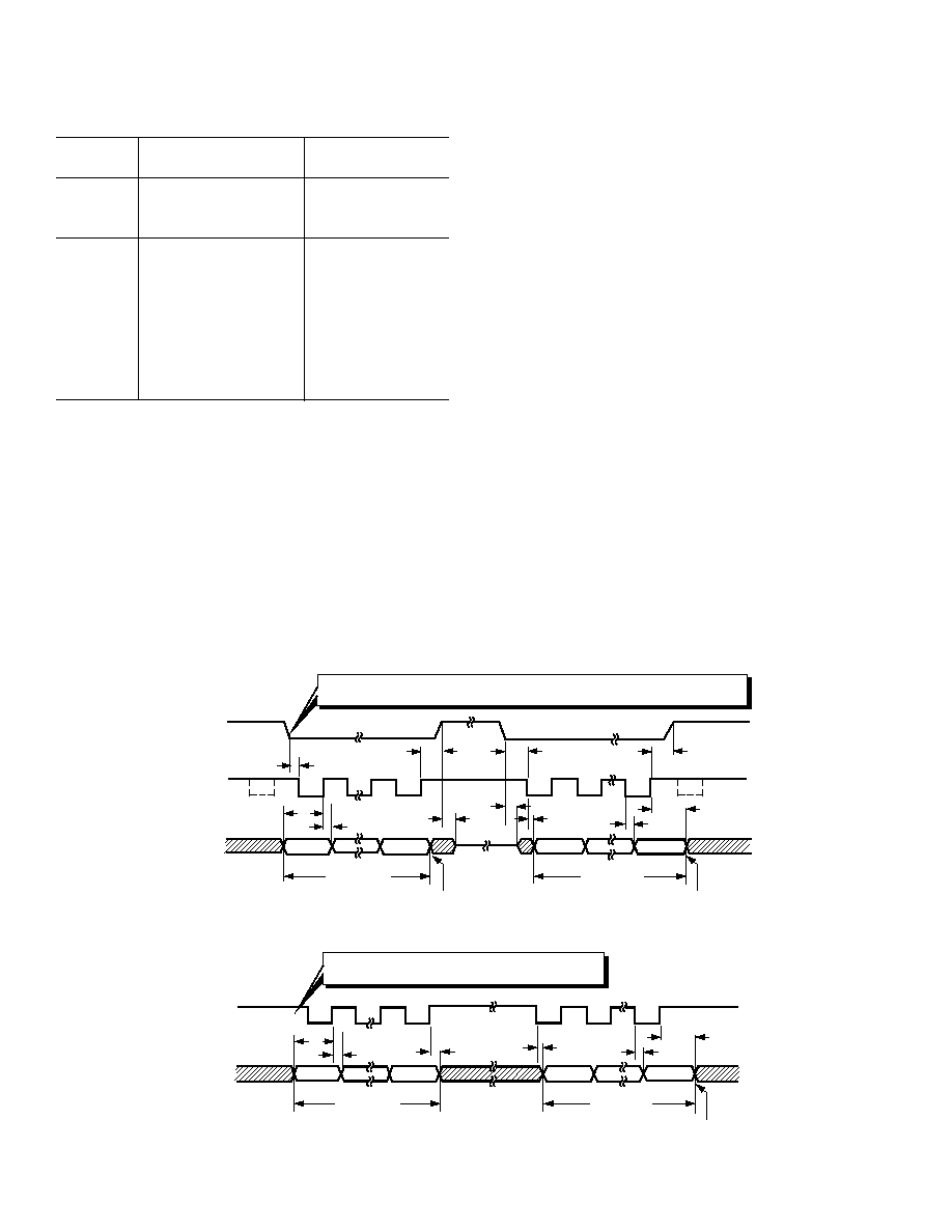
Figures 31 and 32 show the timing diagrams for Operating
Mode 1 in Table X where the AD7856 is in the 2-wire interface
mode. Here the DIN pin is used for both input and output as
shown. The
SYNC input is level-triggered active low and can be
pulsed (Figure 31) or can be constantly low (Figure 32).
In Figure 31 the part samples the input data on the rising edge
of SCLK. After the 16th rising edge of SCLK the DIN is con-
figured as an output. When the
SYNC is taken high the DIN is
three-stated. Taking
SYNC low disables the three-state on the
DIN pin and the first SCLK falling edge clocks out the first data
bit. Once the 16 clocks have been provided the DIN pin will
automatically revert back to an input after a time, t14. Note that
a continuous SCLK shown by the dotted waveform in Figure 31
can be used provided that the
SYNC is low for only 16 clock
pulses in each of the read and write cycles.
In Figure 32 the
SYNC line is permanently tied low and this
results in a different timing arrangement. With
SYNC perma-
nently tied low the DIN pin will never be three-stated. The 16th
rising edge of SCLK configures the DIN pin as an input or an
output as shown in the diagram. Here no more than 16 SCLK
pulses must occur for each of the read and write operations.
If reading from and writing to the calibration registers in this
interface mode, all the selected calibration registers must be
read from or written to. The read and write operations cannot
be aborted. When reading from the calibration registers, the
DIN pin will remain as an output for the full duration of all the
calibration register read operations. When writing to the calibra-
tion registers, the DIN pin will remain as an input for the full
duration of all the calibration register write operations.
NOTE: Initiating conversions in software is not recommended
in Mode 1 operation.
A degradation of 0.3 LSB in linearity can be expected when
operating in Mode 1; however, when hardware initiation of
conversions is used, all other specifications that apply to Mode 2
operation also apply to Mode 1.
t3 = –0.4tSCLK MIN (NONCONTINUOUS SCLK) –/+ 0.4tSCLK ns MIN/MAX (CONTINUOUS SCLK),
t6 = 45/75ns MAX (A/K), t7 = 30/40ns MIN (A/K), t8 = 20ns MIN
POLARITY PIN LOGIC HIGH
SYNC (I/P)
SCLK (I/P)
DIN (I/O)
t3
t11
t3
t11
16
1
16
1
t12
t8
t6
t5
t14
DIN BECOMES AN OUTPUT
DIN BECOMES AN INPUT
DB15
DB0
DB15
DB0
3-STATE
DATA WRITE
DATA READ
t7
Figure 31. Timing Diagram for Read/Write Operation with DIN as an Input/Output (i.e., Mode 1)
POLARITY PIN LOGIC HIGH
SCLK (I/P)
DIN (I/O)
16
1
16
1
t13
t8
t6
t14
DIN BECOMES AN INPUT
DB15
DB0
DB15
DB0
6
t6 = 45/75ns MAX (A/K), t7 = 30/40ns MIN (A/K), t8 = 20ns MIN,
t13 = 90ns MAX, t14 = 50ns MIN
t7
DATA WRITE
DATA READ
Figure 32. Timing Diagram for Read/Write Operation with DIN as an Input/Output and
SYNC Input Tied Low (i.e., Interface Mode 1)
相关PDF资料 |
PDF描述 |
|---|---|
| LTC2392CLX-16#PBF | IC ADC 16BIT SER/PAR 500K 48LQFP |
| ADM3078EYRZ-REEL7 | TXRX 3V 15KV 500KBPS ESD 8-SOIC |
| AD7572AJRZ10 | IC ADC 12BIT HS LC2MOS 24SOIC |
| ADM211EARU-REEL | IC TXRX RS-232 5V 0.1UF 28TSSOP |
| ADM207EARU-REEL | IC TXRX RS232 5DVR/3REC 24TSSOP |
相关代理商/技术参数 |
参数描述 |
|---|---|
| AD7858 | 制造商:AD 制造商全称:Analog Devices 功能描述:3 V to 5 V Single Supply, 200 kSPS 8-Channel, 12-Bit Sampling ADC |
| AD7858AN | 功能描述:IC ADC 12BIT 8CH SRL 24-DIP RoHS:否 类别:集成电路 (IC) >> 数据采集 - 模数转换器 系列:- 标准包装:1 系列:- 位数:14 采样率(每秒):83k 数据接口:串行,并联 转换器数目:1 功率耗散(最大):95mW 电压电源:双 ± 工作温度:0°C ~ 70°C 安装类型:通孔 封装/外壳:28-DIP(0.600",15.24mm) 供应商设备封装:28-PDIP 包装:管件 输入数目和类型:1 个单端,双极 |
| AD7858ANZ | 功能描述:IC ADC 12BIT 8CHAN SRL 24-DIP RoHS:是 类别:集成电路 (IC) >> 数据采集 - 模数转换器 系列:- 标准包装:1,000 系列:- 位数:12 采样率(每秒):300k 数据接口:并联 转换器数目:1 功率耗散(最大):75mW 电压电源:单电源 工作温度:0°C ~ 70°C 安装类型:表面贴装 封装/外壳:24-SOIC(0.295",7.50mm 宽) 供应商设备封装:24-SOIC 包装:带卷 (TR) 输入数目和类型:1 个单端,单极;1 个单端,双极 |
| AD7858AR | 功能描述:IC ADC 12BIT 8CH SRL 24-SOIC RoHS:否 类别:集成电路 (IC) >> 数据采集 - 模数转换器 系列:- 标准包装:1,000 系列:- 位数:12 采样率(每秒):300k 数据接口:并联 转换器数目:1 功率耗散(最大):75mW 电压电源:单电源 工作温度:0°C ~ 70°C 安装类型:表面贴装 封装/外壳:24-SOIC(0.295",7.50mm 宽) 供应商设备封装:24-SOIC 包装:带卷 (TR) 输入数目和类型:1 个单端,单极;1 个单端,双极 |
| AD7858AR-REEL | 制造商:Analog Devices 功能描述:ADC Single SAR 200ksps 12-bit Serial 24-Pin SOIC W T/R 制造商:Analog Devices 功能描述:ADC SGL SAR 200KSPS 12-BIT SERL 24SOIC W - Tape and Reel 制造商:Rochester Electronics LLC 功能描述:SELF CAL.SERIAL 8CH. 12-BIT ADC I.C. - Tape and Reel |
发布紧急采购,3分钟左右您将得到回复。