- 您现在的位置:买卖IC网 > PDF目录10543 > AD7898ARZ-3 (Analog Devices Inc)IC ADC 12BIT SRL HS 5V 8SOIC PDF资料下载
参数资料
| 型号: | AD7898ARZ-3 |
| 厂商: | Analog Devices Inc |
| 文件页数: | 3/16页 |
| 文件大小: | 0K |
| 描述: | IC ADC 12BIT SRL HS 5V 8SOIC |
| 标准包装: | 1 |
| 位数: | 12 |
| 采样率(每秒): | 220k |
| 数据接口: | 串行 |
| 转换器数目: | 1 |
| 功率耗散(最大): | 22.5mW |
| 电压电源: | 单电源 |
| 工作温度: | -40°C ~ 85°C |
| 安装类型: | 表面贴装 |
| 封装/外壳: | 8-SOIC(0.154",3.90mm 宽) |
| 供应商设备封装: | 8-SO |
| 包装: | 管件 |
| 输入数目和类型: | 1 个单端,双极 |
–11–
REV. A
AD7898
CONVST
SCLK
SERIAL READ
OPERATION
CONVERSION
ENDS
3.3 s LATER
OUTPUT
SERIAL
SHIFT
REGISTER
IS RESET
CONVERSION IS
INITIATED AND
TRACK/HOLD GOES INTO
HOLD
READ OPERATION
SHOULD END
100ns
PRIOR TO NEXT
FALLING EDGE OF
CONVST
116
t1
tCONVERT = 3.3 s
100ns MIN
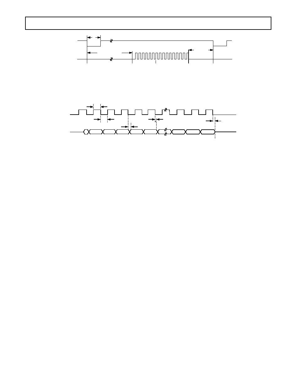
Figure 6. Serial Interface Timing Diagram Mode 0
ZERO
DB11
DB10
DB2
DB0
Z
DB1
ZERO
SDATA
FOUR LEADING ZEROS
THREE-STATE
SCLK
1
5
15
23
4
16
14
t2
t3
t5
t4
t6
Figure 7. Data Read Operation in Mode 0
Figure 7 shows the timing diagram for the read operation to the
AD7898 in Mode 0. The serial clock input (SCLK) provides
the clock source for the serial interface. Serial data is clocked
out from the SDATA line on the falling edge of this clock and is
valid on both the rising and falling edges of SCLK, depending
on the SCLK frequency used. The advantage of having the data
valid on both the rising and falling edges of the SCLK is that it
gives the user greater flexibility in interfacing to the part and
allows a wider range of microprocessor and microcontroller
interfaces to be accommodated. This also explains the two
timing figures, t4 and t5, that are quoted on the diagram.
The time, t4, specifies how long after the falling edge of the
SCLK the next data bit becomes valid, whereas the time, t5,
specifies for how long after the falling edge of the SCLK the
current data bit is valid. The first leading zero is clocked out on
the first rising edge of SCLK. Note that the first leading zero
will be valid on the first falling edge of SCLK even though the
data access time is specified at t4 for the other bits (see Timing
Specifications). The reason the first bit will be clocked out faster
than the other bits is due to the internal architecture of the part.
Sixteen clock pulses must be provided to the part to access to
full conversion result. The AD7898 provides four leading zeros,
followed by the 12-bit conversion result starting with the MSB
(DB11). The last data bit to be clocked out on the 15th fall-
ing clock edge is the LSB (DB0). On the 16th falling edge of
SCLK, the LSB (DB0) will be valid for a specified time to allow
the bit to be read on the falling edge of the SCLK, then the
SDATA line is disabled (three-stated). After this last bit has
been clocked out, the SCLK input should return low and remain
low until the next serial data read operation. If there are extra
clock pulses after the 16th clock, the AD7898 will start over,
outputting data from its output register, and the data bus will no
longer be three-stated even when the clock stops. Provided the
serial clock has stopped before the next falling edge of
CONVST,
the AD7898 will continue to operate correctly with the output
shift register being reset on the falling edge of
CONVST. How-
ever, the SCLK line must be low when
CONVST goes low in
order to correctly reset the output shift register.
The 16 serial clock input does not have to be continuous during
the serial read operation. The 16 bits of data (four leading zeros
and 12-bit conversion result) can be read from the AD7898 in a
number of bytes.
The AD7898 counts the serial clock edges to know which bit
from the output register should be placed on the SDATA out-
put. To ensure that the part does not lose synchronization, the
serial clock counter is reset on the falling edge of the
CONVST
input, provided the SCLK line is low. The user should ensure
that the SCLK line remains low until the end of the conversion.
When the conversion is complete, the output register will be
loaded with the new conversion result and can be read from the
ADC with 16 clock cycles of SCLK.
相关PDF资料 |
PDF描述 |
|---|---|
| VI-2TJ-IW-F2 | CONVERTER MOD DC/DC 36V 100W |
| MC1413DG | IC TRANS ARRAY NPN DARL 16-SOIC |
| TP050F223Z-A-B | CAP CER 0.022UF 25V AXIAL |
| AD7450ABRMZ | IC ADC 12BIT DIFF IN 1MSPS 8MSOP |
| AD7450BRZ | IC ADC 12BIT DIFF IN 1MSPS 8SOIC |
相关代理商/技术参数 |
参数描述 |
|---|---|
| AD7899AR-1 | 功能描述:IC ADC 14BIT 400KSPS 5V 28-SOIC RoHS:否 类别:集成电路 (IC) >> 数据采集 - 模数转换器 系列:- 标准包装:1,000 系列:- 位数:12 采样率(每秒):300k 数据接口:并联 转换器数目:1 功率耗散(最大):75mW 电压电源:单电源 工作温度:0°C ~ 70°C 安装类型:表面贴装 封装/外壳:24-SOIC(0.295",7.50mm 宽) 供应商设备封装:24-SOIC 包装:带卷 (TR) 输入数目和类型:1 个单端,单极;1 个单端,双极 |
| AD7899AR-1REEL | 制造商:Analog Devices 功能描述:ADC Single SAR 400ksps 14-bit Parallel 28-Pin SOIC W T/R |
| AD7899AR-1REEL7 | 制造商:Analog Devices 功能描述:ADC SGL SAR 400KSPS 14BIT PARALLEL 28SOIC W - Tape and Reel |
| AD7899AR-2 | 功能描述:IC ADC 14BIT 400KSPS 5V 28-SOIC RoHS:否 类别:集成电路 (IC) >> 数据采集 - 模数转换器 系列:- 产品培训模块:Lead (SnPb) Finish for COTS Obsolescence Mitigation Program 标准包装:2,500 系列:- 位数:12 采样率(每秒):3M 数据接口:- 转换器数目:- 功率耗散(最大):- 电压电源:- 工作温度:- 安装类型:表面贴装 封装/外壳:SOT-23-6 供应商设备封装:SOT-23-6 包装:带卷 (TR) 输入数目和类型:- |
| AD7899AR-2REEL | 制造商:Analog Devices 功能描述:ADC Single SAR 400ksps 14-bit Parallel 28-Pin SOIC W T/R |
发布紧急采购,3分钟左右您将得到回复。