- 您现在的位置:买卖IC网 > PDF目录10543 > AD7898ARZ-3 (Analog Devices Inc)IC ADC 12BIT SRL HS 5V 8SOIC PDF资料下载
参数资料
| 型号: | AD7898ARZ-3 |
| 厂商: | Analog Devices Inc |
| 文件页数: | 7/16页 |
| 文件大小: | 0K |
| 描述: | IC ADC 12BIT SRL HS 5V 8SOIC |
| 标准包装: | 1 |
| 位数: | 12 |
| 采样率(每秒): | 220k |
| 数据接口: | 串行 |
| 转换器数目: | 1 |
| 功率耗散(最大): | 22.5mW |
| 电压电源: | 单电源 |
| 工作温度: | -40°C ~ 85°C |
| 安装类型: | 表面贴装 |
| 封装/外壳: | 8-SOIC(0.154",3.90mm 宽) |
| 供应商设备封装: | 8-SO |
| 包装: | 管件 |
| 输入数目和类型: | 1 个单端,双极 |
–15–
REV. A
AD7898
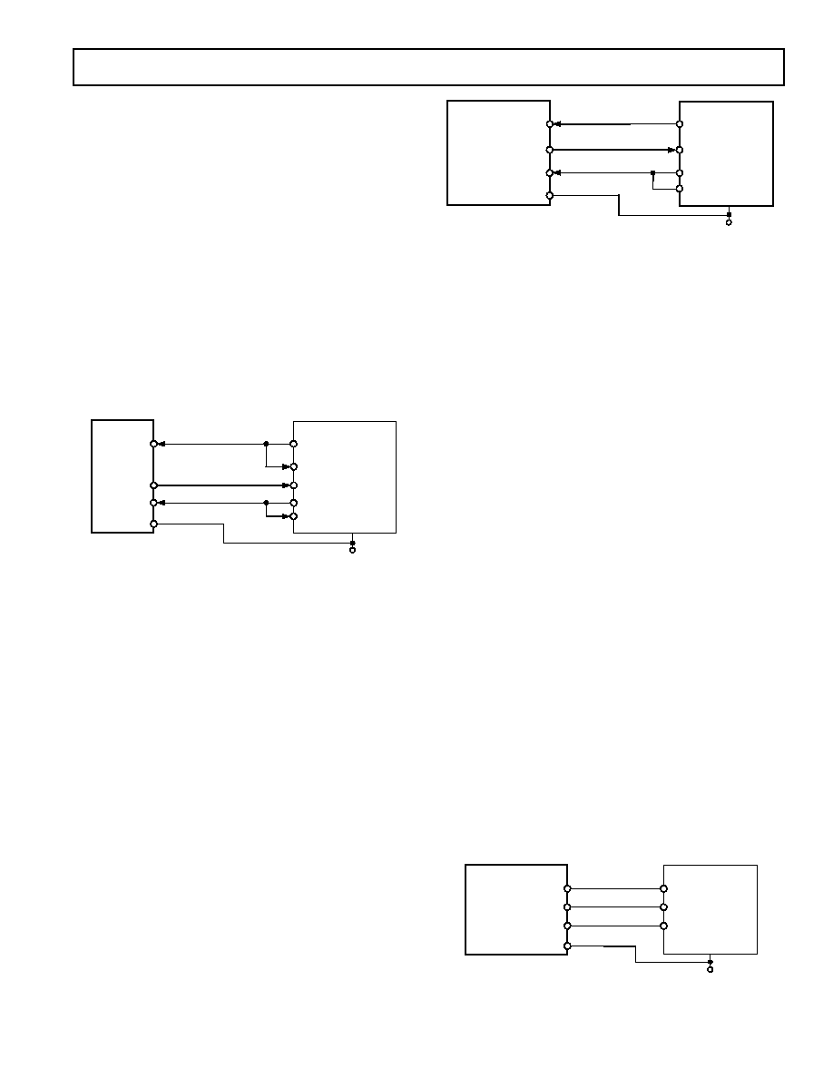
TMS320C5x/C54x to AD7898 Interface
The serial interface on the TMS320C5x/C54x uses a continu-
ous serial clock and frame synchronization signal to synchronize
the data transfer operations with peripheral devices like the
AD7898. The
CS input allows easy interfacing between the
TMS320C5x/C54x and the AD7898 without any glue logic
required. The serial port of the TMS320C5x/C54x is set up to
operate in burst mode with internal CLKX (TX serial clock)
and FSX (TX frame sync). The serial port control register (SPC)
must have the following setup: FO = 0, FSM = 1, MCM = 1,
and TXM = 1. The format bit, FO, may be set to 1 to set the
word length to 8 bits, in order to implement the power-down
modes on the AD7898.
The connection diagram is shown in Figure 17. It should be
noted that for signal processing applications, it is imperative that
the frame synchronization signal from the TMS320C5x/C54x
will provide equidistant sampling. The VDRIVE pin of the AD7898
takes the same supply voltage as that of the TMS320C5x/C54x.
This allows the ADC to operate at a higher voltage than the
serial interface, i.e., TMS320C5x/C54x, if necessary.
AD7898*
SDATA
SCLK
CS
TMS320C5x/C54x*
*ADDITIONAL PINS OMITTED FOR CLARITY
CLKX
CLKR
DR
FSX
FSR
VDRIVE
VDD
Figure 17. AD7898 to TMS320C5x Interface
AD7898 to ADSP-21xx Interface
The ADSP-21xx family of DSPs are interfaced directly to the
AD7898 without any glue logic required. The VDRIVE pin of the
AD7898 takes the same supply voltage as that of the ADSP-21xx.
This allows the ADC to operate at a higher voltage than the
serial interface, i.e., ADSP-21xx, if necessary.
The SPORT control register should be set up as follows:
TFSW = RFSW = 1, Alternate Framing
INVRFS = INVTFS = 1, Active Low Frame Signal
DTYPE = 00, Right Justify Data
SLEN = 1111, 16-Bit Data Words
ISCLK = 1, Internal Serial Clock
TFSR = RFSR = 1, Frame Every Word
IRFS = 0,
ITFS = 1.
To implement the power-down mode, SLEN should be set to
1001 to issue an 8-bit SCLK burst.
The connection diagram is shown in Figure 18. The ADSP-21xx
has the TFS and RFS of the SPORT tied together, with TFS
set as an output and RFS set as an input. The DSP operates in
Alternate Framing Mode and the SPORT control register is set
up as described. The Frame Synchronization signal generated
on the TFS is tied to
CS and as with all signal processing applica-
tions equidistant sampling is necessary. However, in this example,
the timer interrupt is used to control the sampling rate of the
ADC and, under certain conditions, equidistant sampling may
not be achieved.
AD7898*
SCLK
CS
SDATA
VDRIVE
ADSP-21xx*
*ADDITIONAL PINS OMITTED FOR CLARITY
SCLK
DR
RFS
TFS
VDD
Figure 18. AD7898 to ADSP-21xx Interface
The Timer registers, among other things, are loaded with a value
that will provide an interrupt at the required sample interval.
When an interrupt is received, a value is transmitted with
TFS/DT (ADC control word). The TFS is used to control the
RFS and hence the reading of data. The frequency of the serial
clock is set in the SCLKDIV register. When the instruction to
transmit with TFS is given, (i.e., AX0 = TX0), the state of the
SCLK is checked. The DSP will wait until the SCLK has gone
high, low and high before transmission will start. If the timer
and SCLK values are chosen such that the instruction to trans-
mit occurs on or near the rising edge of SCLK, then the data
may be transmitted or it may wait until the next clock edge.
For example, the ADSP-2111 has a master clock frequency of
16 MHz. If the SCLKDIV register is loaded with the value 3, a
SCLK of 2 MHz is obtained, and eight master clock periods will
elapse for every 1 SCLK period. If the timer registers are loaded
with the value 803, 100.5 SCLKs will occur between interrupts
and subsequently between transmit instructions. This situation
will result in nonequidistant sampling as the transmit instruction
is occurring on an SCLK edge. If the number of SCLKs between
interrupts is a whole integer figure of N, equidistant sampling
will be implemented by the DSP.
AD7898 to DSP56xxx Interface
The connection diagram in Figure 19 shows how the AD7898
can be connected to the SSI (Synchronous Serial Interface) of
the DSP56xxx family of DSPs from Motorola. The SSI is oper-
ated in Synchronous Mode (SYN bit in CRB = 1) with internally
generated 1-bit clock period frame sync for both TX and RX
(bits FSL1 = 1 and FSL0 = 0 in CRB). Set the word length to
16 by setting bits WL1 = 1 and WL0 = 0 in CRA. To implement
the power-down mode on the AD7898 then the word length
can be changed to 8 bits by setting bits WL1 = 0 and WL0 = 0
in CRA. It should be noted that for signal processing applica-
tions, it is imperative that the frame synchronization signal
from the DSP56xxx will provide equidistant sampling. The
VDRIVE pin of the AD7898 takes the same supply voltage as that
of the DSP56xxx. This allows the ADC to operate at a higher
voltage than the serial interface, i.e., DSP56xxx, if necessary.
AD7898*
SDATA
SCLK
CS
DSP56xxx*
*ADDITIONAL PINS OMITTED FOR CLARITY
SCK
SRD
SC2
VDRIVE
VDD
Figure 19. AD7898 to DSP56xxx Interface
相关PDF资料 |
PDF描述 |
|---|---|
| VI-2TJ-IW-F2 | CONVERTER MOD DC/DC 36V 100W |
| MC1413DG | IC TRANS ARRAY NPN DARL 16-SOIC |
| TP050F223Z-A-B | CAP CER 0.022UF 25V AXIAL |
| AD7450ABRMZ | IC ADC 12BIT DIFF IN 1MSPS 8MSOP |
| AD7450BRZ | IC ADC 12BIT DIFF IN 1MSPS 8SOIC |
相关代理商/技术参数 |
参数描述 |
|---|---|
| AD7899AR-1 | 功能描述:IC ADC 14BIT 400KSPS 5V 28-SOIC RoHS:否 类别:集成电路 (IC) >> 数据采集 - 模数转换器 系列:- 标准包装:1,000 系列:- 位数:12 采样率(每秒):300k 数据接口:并联 转换器数目:1 功率耗散(最大):75mW 电压电源:单电源 工作温度:0°C ~ 70°C 安装类型:表面贴装 封装/外壳:24-SOIC(0.295",7.50mm 宽) 供应商设备封装:24-SOIC 包装:带卷 (TR) 输入数目和类型:1 个单端,单极;1 个单端,双极 |
| AD7899AR-1REEL | 制造商:Analog Devices 功能描述:ADC Single SAR 400ksps 14-bit Parallel 28-Pin SOIC W T/R |
| AD7899AR-1REEL7 | 制造商:Analog Devices 功能描述:ADC SGL SAR 400KSPS 14BIT PARALLEL 28SOIC W - Tape and Reel |
| AD7899AR-2 | 功能描述:IC ADC 14BIT 400KSPS 5V 28-SOIC RoHS:否 类别:集成电路 (IC) >> 数据采集 - 模数转换器 系列:- 产品培训模块:Lead (SnPb) Finish for COTS Obsolescence Mitigation Program 标准包装:2,500 系列:- 位数:12 采样率(每秒):3M 数据接口:- 转换器数目:- 功率耗散(最大):- 电压电源:- 工作温度:- 安装类型:表面贴装 封装/外壳:SOT-23-6 供应商设备封装:SOT-23-6 包装:带卷 (TR) 输入数目和类型:- |
| AD7899AR-2REEL | 制造商:Analog Devices 功能描述:ADC Single SAR 400ksps 14-bit Parallel 28-Pin SOIC W T/R |
发布紧急采购,3分钟左右您将得到回复。