- 您现在的位置:买卖IC网 > PDF目录10212 > AD7952BSTZRL (Analog Devices Inc)IC ADC 14BIT DIFF 1MSPS 48-LQFP PDF资料下载
参数资料
| 型号: | AD7952BSTZRL |
| 厂商: | Analog Devices Inc |
| 文件页数: | 14/32页 |
| 文件大小: | 0K |
| 描述: | IC ADC 14BIT DIFF 1MSPS 48-LQFP |
| 标准包装: | 2,000 |
| 系列: | PulSAR® |
| 位数: | 14 |
| 采样率(每秒): | 1M |
| 数据接口: | 并联 |
| 转换器数目: | 1 |
| 功率耗散(最大): | 260mW |
| 电压电源: | 模拟和数字,双 ± |
| 工作温度: | -40°C ~ 85°C |
| 安装类型: | 表面贴装 |
| 封装/外壳: | 48-LQFP |
| 供应商设备封装: | 48-LQFP(7x7) |
| 包装: | 带卷 (TR) |
| 输入数目和类型: | 1 个差分,双极 |
第1页第2页第3页第4页第5页第6页第7页第8页第9页第10页第11页第12页第13页当前第14页第15页第16页第17页第18页第19页第20页第21页第22页第23页第24页第25页第26页第27页第28页第29页第30页第31页第32页
Data Sheet
AD7952
Rev. A | Page 21 of 32
DRIVER AMPLIFIER CHOICE
Although the AD7952 is easy to drive, the driver amplifier must
meet the following requirements:
For multichannel, multiplexed applications, the driver
amplifier and the AD7952 analog input circuit must be
able to settle for a full-scale step of the capacitor array at a
14-bit level (0.006%). For the amplifier, settling at 0.1% to
0.01% is more commonly specified. This differs significantly
from the settling time at a 14-bit level and should be
verified prior to driver selection. The AD8021 op amp com-
bines ultralow noise and high gain bandwidth and meets
this settling time requirement even when used with gains
of up to 13.
The noise generated by the driver amplifier needs to be
kept as low as possible to preserve the SNR and transition
noise performance of the AD7952. The noise coming from
the driver is filtered by the external 1-pole, low-pass filter,
as shown in Figure 27. The SNR degradation due to the
amplifier is
2
3dB
2
3dB
2
)
(
f
2
)
(
f
2
log
20
N
NADC
LOSS
Ne
V
SNR
where:
VNADC is the noise of the ADC, which is:
20
10
2
SNR
INp-p
NADC
V
f–3dB is the cutoff frequency of the input filter (3.9 MHz).
N is the noise factor of the amplifier (1 in the buffer
configuration).
eN+ and eN are the equivalent input voltage noise densities
of the op amps connected to IN+ and IN, in nV/√Hz.
When the resistances used around the amplifiers are small,
this approximation can be used. If larger resistances are
used, their noise contributions should also be root-sum
squared.
The driver needs to have a THD performance suitable to
that of the AD7952. Figure 15 shows the THD vs. frequency
that the driver should exceed.
The AD8021 meets these requirements and is appropriate for
almost all applications. The AD8021 needs a 10 pF external
compensation capacitor that should have good linearity as an
NPO ceramic or mica type. Moreover, the use of a noninverting
+1 gain arrangement is recommended and helps to obtain the
best SNR.
The AD8022 can also be used when a dual version is needed
and a gain of 1 is present. The AD829 is an alternative in
applications where high frequency performance (above 100 kHz)
is not required. In applications with a gain of 1, an 82 pF
compensation capacitor is required. The AD8610 is an option
when low bias current is needed in low frequency applications.
Because the AD7952 uses a large geometry, high voltage input
switch, the best linearity performance is obtained when using
the amplifier at its maximum full power bandwidth. Gaining
the amplifier to make use of the more dynamic range of the
ADC results in increased linearity errors. For applications
requiring more resolution, the use of an additional amplifier
with gain should precede a unity follower driving the AD7952.
See Table 8 for a list of recommended op amps.
Table 8. Recommended Driver Amplifiers
Amplifier
Typical Application
±15 V supplies, very low noise, low frequency
±12 V supplies, very low noise, high frequency
±12 V supplies, very low noise, high
frequency, dual
±12 V supplies, low noise, high frequency,
single-ended-to-differential driver
±13 V supplies, low bias current, low
frequency, single/dual
Single-to-Differential Driver
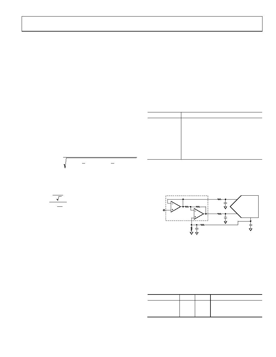
For single-ended sources, a single-to-differential driver, such
as the ADA4922-1, can be used because the AD7952 needs to
be driven differentially. The 1-pole filter using R = 15 Ω and
C = 2.7 nF provides a corner frequency of 3.9 MHz.
0
6589
-047
ANALOG
INPUT
IN+
IN–
AD7952
REF
10F
15
100nF
2.7nF
U2
R1
R2
ADA4922-1
OUT+
VCC
VEE
OUT–
IN
REF
RF
RG
Figure 30. Single-to-Differential Driver Using the ADA4922-1
For unipolar 5 V and 10 V input ranges, the internal (or
external) reference source can be used to level shift U2 for
the correct input span. If using an external reference, the
values for R1/R2 can be lowered to reduce resistive Johnson
noise (1.29E 10 × √R). For the bipolar ±5 V and ±10 V input
ranges, the reference connection is not required because the
common-mode voltage is 0 V. See Table 9 for R1/R2 for the
different input ranges.
Table 9. R1/R2 Configuration
Input Range (V)
R1 (Ω)
R2 (Ω)
Common-ModeVoltage (V)
5
2.5 k
2.5
10
2.5 k
Open
5
±5, ±10
100
0
相关PDF资料 |
PDF描述 |
|---|---|
| LTC2280CUP#TRPBF | IC ADC DUAL 10BIT 105MSPS 64-QFN |
| SP3084EEN-L/TR | IC TXRX RS485/RS422 ESD 8NSOIC |
| AD7357BRUZ-RL | IC ADC 14BITDUAL 4.MSPS 16TSSOP |
| SP3083EEN-L/TR | IC TXRX RS485/RS422 ESD 14NSOIC |
| SP3081EEN-L/TR | IC TXRX RS485/RS422 ESD 8NSOIC |
相关代理商/技术参数 |
参数描述 |
|---|---|
| AD795AH | 制造商:未知厂家 制造商全称:未知厂家 功能描述:Voltage-Feedback Operational Amplifier |
| AD795BH | 制造商:未知厂家 制造商全称:未知厂家 功能描述:Voltage-Feedback Operational Amplifier |
| AD795JN | 制造商:Analog Devices 功能描述:Operational Amplifier, Single AMP, Bipolar/JFET, 8 Pin, Plastic, DIP |
| AD795JR | 功能描述:IC OPAMP JFET 1.6MHZ LN 8SOIC RoHS:否 类别:集成电路 (IC) >> Linear - Amplifiers - Instrumentation 系列:- 标准包装:2,500 系列:Excalibur™ 放大器类型:J-FET 电路数:1 输出类型:- 转换速率:45 V/µs 增益带宽积:10MHz -3db带宽:- 电流 - 输入偏压:20pA 电压 - 输入偏移:490µV 电流 - 电源:1.7mA 电流 - 输出 / 通道:48mA 电压 - 电源,单路/双路(±):4.5 V ~ 38 V,±2.25 V ~ 19 V 工作温度:-40°C ~ 85°C 安装类型:表面贴装 封装/外壳:8-SOIC(0.154",3.90mm 宽) 供应商设备封装:8-SOIC 包装:带卷 (TR) |
| AD795JR-REEL | 功能描述:IC OPAMP JFET 1.6MHZ LN 8SOIC RoHS:否 类别:集成电路 (IC) >> Linear - Amplifiers - Instrumentation 系列:- 标准包装:50 系列:- 放大器类型:J-FET 电路数:2 输出类型:- 转换速率:13 V/µs 增益带宽积:3MHz -3db带宽:- 电流 - 输入偏压:65pA 电压 - 输入偏移:3000µV 电流 - 电源:1.4mA 电流 - 输出 / 通道:- 电压 - 电源,单路/双路(±):7 V ~ 36 V,±3.5 V ~ 18 V 工作温度:-40°C ~ 85°C 安装类型:通孔 封装/外壳:8-DIP(0.300",7.62mm) 供应商设备封装:8-PDIP 包装:管件 |
发布紧急采购,3分钟左右您将得到回复。