- 您现在的位置:买卖IC网 > PDF目录10212 > AD7952BSTZRL (Analog Devices Inc)IC ADC 14BIT DIFF 1MSPS 48-LQFP PDF资料下载
参数资料
| 型号: | AD7952BSTZRL |
| 厂商: | Analog Devices Inc |
| 文件页数: | 22/32页 |
| 文件大小: | 0K |
| 描述: | IC ADC 14BIT DIFF 1MSPS 48-LQFP |
| 标准包装: | 2,000 |
| 系列: | PulSAR® |
| 位数: | 14 |
| 采样率(每秒): | 1M |
| 数据接口: | 并联 |
| 转换器数目: | 1 |
| 功率耗散(最大): | 260mW |
| 电压电源: | 模拟和数字,双 ± |
| 工作温度: | -40°C ~ 85°C |
| 安装类型: | 表面贴装 |
| 封装/外壳: | 48-LQFP |
| 供应商设备封装: | 48-LQFP(7x7) |
| 包装: | 带卷 (TR) |
| 输入数目和类型: | 1 个差分,双极 |
第1页第2页第3页第4页第5页第6页第7页第8页第9页第10页第11页第12页第13页第14页第15页第16页第17页第18页第19页第20页第21页当前第22页第23页第24页第25页第26页第27页第28页第29页第30页第31页第32页
Data Sheet
AD7952
Rev. A | Page 29 of 32
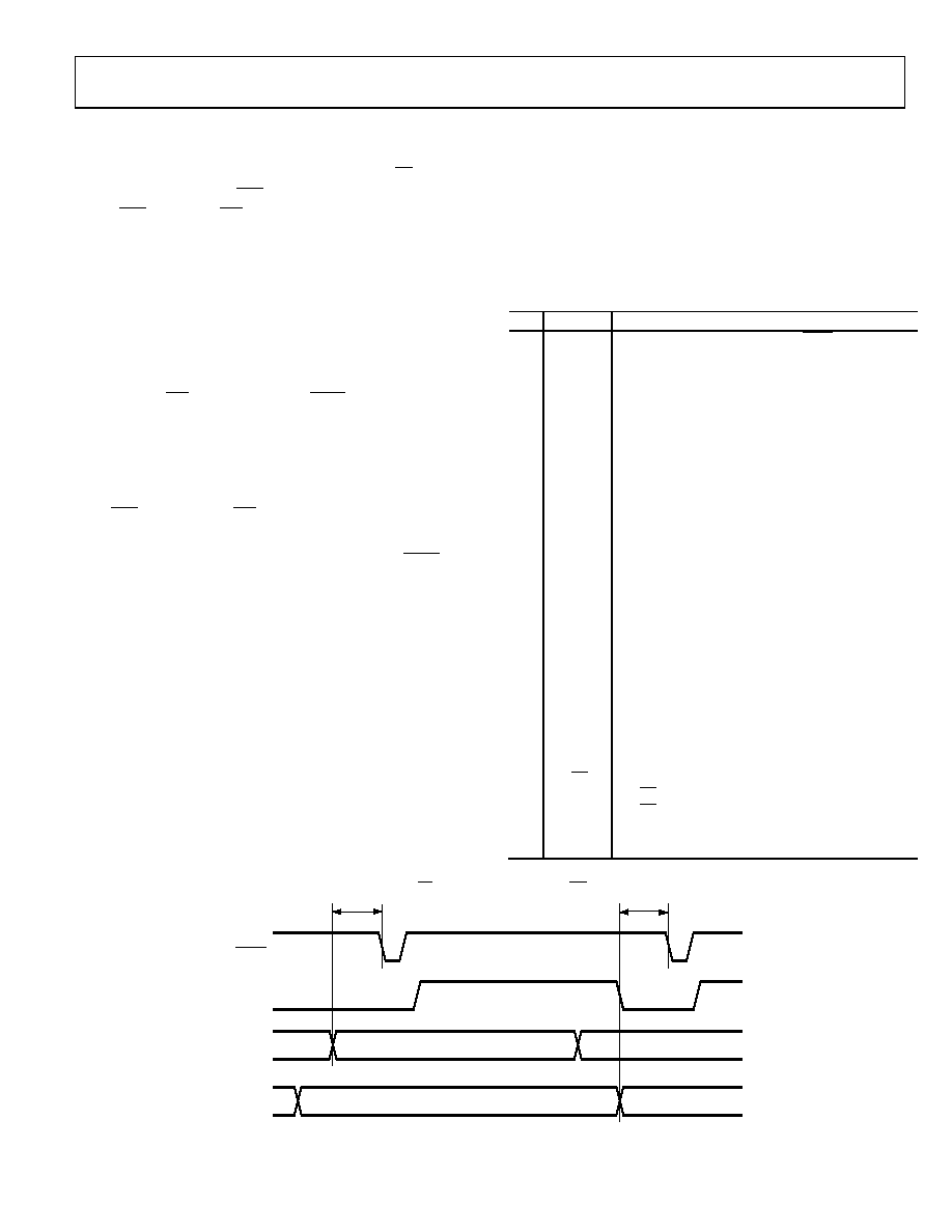
HARDWARE CONFIGURATION
The AD7952 can be configured at any time with the dedicated
hardware pins WARP, IMPULSE, BIPOLAR, TEN, OB/2C, and
PD for parallel mode (SER/PAR = low) or serial hardware mode
(SER/ PAR = high, HW/SW = high). Programming the AD7952
for mode selection and input range configuration can be done
before or during conversion. Like the RESET input, the ADC
requires at least one acquisition time to settle, as shown in
Figure 45. See Table 6 for pin descriptions. Note that these
inputs are high impedance when using the software
configuration mode.
SOFTWARE CONFIGURATION
The pins multiplexed on D[13:10] used for software configura-
tion are: HW/SW, SCIN, SCCLK, and SCCS. The AD7952 is
programmed using the dedicated write-only serial configurable
port (SCP) for conversion mode, input range selection, output
coding, and power-down using the serial configuration register.
See Table 10 for details of each bit in the configuration register.
The SCP can only be used in serial software mode selected with
SER/PAR = high and HW/SW = low because the port is
multiplexed on the parallel interface.
The SCP is accessed by asserting the port’s chip select, SCCS,
and then writing SCIN synchronized with SCCLK, which (like
SDCLK) is edge sensitive depending on the state of INVSCLK.
See Figure 46 for timing details. SCIN is clocked into the con-
figuration register MSB first. The configuration register is an
internal shift register that begins with Bit 8, the START bit. The
9th SPPCLK edge updates the register and allows the new settings to
be used. As indicated in the timing diagram, at least one acquisition
time is required from the 9th SCCLK edge. Bits [1:0] are reserved
bits and are not written to while the SCP is being updated.
The SCP can be written to at any time, up to 40 MHz, and it is
recommended to write to while the AD7952 is not busy
converting, as detailed in Figure 46. In this mode, the full
1 MSPS is not attainable because the time required for SCP access
is (t31 + 9 × 1/SCCLK + t8) minimum. If the full throughput is
required, the SCP can be written to during conversion; however,
it is not recommended to write to the SCP during the last 450 ns
of conversion (BUSY = high), or performance degradation can
result. In addition, the SCP can be accessed in both serial master
and serial slave read during and read after convert modes.
Note that at power-up, the configuration register is undefined.
The RESET input clears the configuration register (sets all bits
to 0), thus placing the configuration to 0 V to 5 V input, normal
mode, and twos complemented output.
Table 10. Configuration Register Description
Bit
Name
Description
8
START
START bit. With the SCP enabled (SCCS = low),
when START is high, the first rising edge of SCCLK
(INVSCLK = low) begins to load the register with the
new configuration.
7
BIPOLAR
Input Range Select. Used in conjunction with Bit 6,
TEN, per the following.
Input Range (V)
BIPOLAR
TEN
0 to 5
Low
0 to 10
Low
High
±5
High
Low
±10
High
6
TEN
Input Range Select. See Bit 7, BIPOLAR.
5
PD
Power Down.
PD = low, normal operation.
PD = high, power down the ADC. The SCP is
accessible while in power-down. To power-up
the ADC, write PD = low on the next configuration
setting.
4
IMPULSE
Mode Select. Used in conjunction with Bit 3, WARP,
per the following.
Mode
WARP
IMPULSE
Normal
Low
Impulse
Low
High
Warp
High
Low
Normal
High
3
WARP
Mode Select. See Bit 4, IMPULSE.
2
OB/2C
Output Coding.
OB/2C = low, use twos complement output.
OB/2C = high, use straight binary output.
1
RSV
Reserved.
0
RSV
Reserved.
WARP,
IMPULSE
BUSY
HW/SW = 0
CNVST
BIPOLAR,
TEN
t8
SER/PAR = 0, 1
PD = 0
t8
0
65
89
-0
44
Figure 45. Hardware Configuration Timing
相关PDF资料 |
PDF描述 |
|---|---|
| LTC2280CUP#TRPBF | IC ADC DUAL 10BIT 105MSPS 64-QFN |
| SP3084EEN-L/TR | IC TXRX RS485/RS422 ESD 8NSOIC |
| AD7357BRUZ-RL | IC ADC 14BITDUAL 4.MSPS 16TSSOP |
| SP3083EEN-L/TR | IC TXRX RS485/RS422 ESD 14NSOIC |
| SP3081EEN-L/TR | IC TXRX RS485/RS422 ESD 8NSOIC |
相关代理商/技术参数 |
参数描述 |
|---|---|
| AD795AH | 制造商:未知厂家 制造商全称:未知厂家 功能描述:Voltage-Feedback Operational Amplifier |
| AD795BH | 制造商:未知厂家 制造商全称:未知厂家 功能描述:Voltage-Feedback Operational Amplifier |
| AD795JN | 制造商:Analog Devices 功能描述:Operational Amplifier, Single AMP, Bipolar/JFET, 8 Pin, Plastic, DIP |
| AD795JR | 功能描述:IC OPAMP JFET 1.6MHZ LN 8SOIC RoHS:否 类别:集成电路 (IC) >> Linear - Amplifiers - Instrumentation 系列:- 标准包装:2,500 系列:Excalibur™ 放大器类型:J-FET 电路数:1 输出类型:- 转换速率:45 V/µs 增益带宽积:10MHz -3db带宽:- 电流 - 输入偏压:20pA 电压 - 输入偏移:490µV 电流 - 电源:1.7mA 电流 - 输出 / 通道:48mA 电压 - 电源,单路/双路(±):4.5 V ~ 38 V,±2.25 V ~ 19 V 工作温度:-40°C ~ 85°C 安装类型:表面贴装 封装/外壳:8-SOIC(0.154",3.90mm 宽) 供应商设备封装:8-SOIC 包装:带卷 (TR) |
| AD795JR-REEL | 功能描述:IC OPAMP JFET 1.6MHZ LN 8SOIC RoHS:否 类别:集成电路 (IC) >> Linear - Amplifiers - Instrumentation 系列:- 标准包装:50 系列:- 放大器类型:J-FET 电路数:2 输出类型:- 转换速率:13 V/µs 增益带宽积:3MHz -3db带宽:- 电流 - 输入偏压:65pA 电压 - 输入偏移:3000µV 电流 - 电源:1.4mA 电流 - 输出 / 通道:- 电压 - 电源,单路/双路(±):7 V ~ 36 V,±3.5 V ~ 18 V 工作温度:-40°C ~ 85°C 安装类型:通孔 封装/外壳:8-DIP(0.300",7.62mm) 供应商设备封装:8-PDIP 包装:管件 |
发布紧急采购,3分钟左右您将得到回复。