- 您现在的位置:买卖IC网 > PDF目录5369 > AD8027ARZ-REEL7 (Analog Devices Inc)IC OPAMP R-R LDIST LN LP 8SOIC PDF资料下载
参数资料
| 型号: | AD8027ARZ-REEL7 |
| 厂商: | Analog Devices Inc |
| 文件页数: | 11/25页 |
| 文件大小: | 0K |
| 描述: | IC OPAMP R-R LDIST LN LP 8SOIC |
| 标准包装: | 1,000 |
| 放大器类型: | 电压反馈 |
| 电路数: | 1 |
| 输出类型: | 满摆幅 |
| 转换速率: | 100 V/µs |
| -3db带宽: | 190MHz |
| 电流 - 输入偏压: | 4µA |
| 电压 - 输入偏移: | 200µV |
| 电流 - 电源: | 6.5mA |
| 电流 - 输出 / 通道: | 120mA |
| 电压 - 电源,单路/双路(±): | 2.7 V ~ 12 V,±1.35 V ~ 6 V |
| 工作温度: | -40°C ~ 125°C |
| 安装类型: | 表面贴装 |
| 封装/外壳: | 8-SOIC(0.154",3.90mm 宽) |
| 供应商设备封装: | 8-SO |
| 包装: | 带卷 (TR) |
AD8027/AD8028
Rev. C | Page 18 of 24
In the event that the crossover region cannot be avoided,
specific attention has been given to the input stage to ensure
constant transconductance and minimal offset in all regions of
operation. The regions are PNP input pair running, NPN input
pair running, and both running at the same time (in the
200 mV crossover region). Maintaining constant transconduc-
tance in all regions ensures the best wideband distortion
performance when going between these regions. With this
technique, the AD8027/AD8028 can achieve greater than 80 dB
SFDR for a 2 V p-p, 1 MHz, and G = 1 signal on ±1.5 V
supplies. Another requirement needed to achieve this level of
distortion is that the offset of each pair must be laser trimmed
to achieve greater than 80 dB SFDR, even for low frequency
signals.
OUTPUT STAGE
The AD8027/AD8028 use a common-emitter output structure
to achieve rail-to-rail output capability. The output stage is
designed to drive 50 mA of linear output current, 40 mA within
200 mV of the rail, and 2.5 mA within 35 mV of the rail.
Loading of the output stage, including any possible feedback
network, lowers the open-loop gain of the amplifier. Refer to
Figure 49 for the loading behavior. Capacitive load can degrade
the phase margin of the amplifier. The AD8027/AD8028 can
drive up to 20 pF, G = 1, as shown in Figure 10. A small (25 Ω
to 50 Ω) series resistor, RSNUB, should be included, if the
capacitive load is to exceed 20 pF for a gain of 1. Increasing the
closed-loop gain increases the amount of capacitive load that
can be driven before a series resistor needs to be included.
B
DC ERRORS
The AD8027/AD8028 use two complementary input stages to
achieve rail-to-rail input performance, as mentioned in the
Input Stage section. To use the dc performance over the entire
common-mode range, the input bias current and input offset
voltage of each pair must be considered.
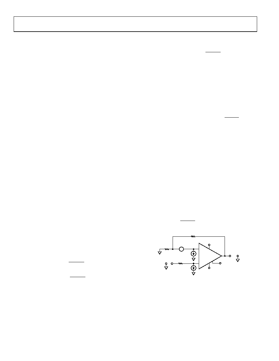
Referring to Figure 56, the output offset voltage of each pair is
calculated by
+
=
G
F
G
PNP
OS
OUT
PNP
OS
R
V
,
+
=
G
F
G
NPN
OS
OUT
NPN
OS
R
V
,
where the difference of the two is the discontinuity experienced
when going through the crossover region.
The size of the discontinuity is defined as
(
)
+
×
=
G
F
G
NPN
OS,
PNP
OS,
DIS
R
V
Using the crossover select feature of the AD8027/AD8028 helps
to avoid this region. In the event that the region cannot be
avoided, the quantity (VOS, PNP – VOS, NPN) is trimmed to minimize
this effect.
Because the input pairs are complementary, the input bias cur-
rent reverses polarity when going through the crossover region
shown in Figure 37. The offset between pairs is described by
()
+
×
=
F
G
F
G
S
NPN
B,
PNP
B,
NPN
OS,
PNP
OS,
R
I
V
IB, PNP is the input bias current of either input when the PNP
input pair is active, and IB, NPN is the input bias current of either
input pair when the NPN pair is active. If RS is sized so that
when multiplied by the gain factor it equals RF, this effect is
eliminated. It is strongly recommended to balance the imped-
ances in this manner when traveling through the crossover
region to minimize the dc error and distortion. As an example,
assuming that the PNP input pair has an input bias current of
6 μA and the NPN input pair has an input bias current of
2 μA, a 200 μV shift in offset occurs when traveling through
the crossover region with RF equal to 0 Ω and RS equal to 25 Ω.
In addition to the input bias current shift between pairs, each
input pair has an input bias current offset that contributes to the
total offset in the following manner:
F
B
G
F
G
S
B
OS
R
I
R
I
V
+
+
=
Δ
VOUT
IB+
RF
RG
IB–
VOS
RS
+–
VI
+
–
SELECT
–V
+V
–
+
AD8027/
AD8028
03327-A-055
Figure 56. Op Amp DC Error Sources
相关PDF资料 |
PDF描述 |
|---|---|
| AD8030ARZ-REEL7 | IC AMP GP R-R DUAL LP 8SOIC |
| 0034.5616.22 | FUSE 800MA 250V TLAG 5X20 SMD TR |
| ADA4930-2YCPZ-R2 | IC DIFF AMP 1.35GHZ 24-LFCSP |
| 0034.5617.22 | FUSE 1A 250V T-LAG 5X20 SMD T/R |
| KTR10EZPF1804 | RES 1.80M OHM 1/8W 1% 0805 SMD |
相关代理商/技术参数 |
参数描述 |
|---|---|
| AD8028 | 制造商:AD 制造商全称:Analog Devices 功能描述:Low Distortion, High Speed Rail-to-Rail Input/Output Amplifiers |
| AD8028AR | 制造商:Rochester Electronics LLC 功能描述:HIGH PERFORMANCE RRIO - Bulk 制造商:Analog Devices 功能描述:AMP LOW DISTORTION RRI/O SMD 8028 |
| AD8028AR-EBZ | 功能描述:BOARD EVAL FOR AD8028AR RoHS:是 类别:编程器,开发系统 >> 评估板 - 运算放大器 系列:- 产品培训模块:Lead (SnPb) Finish for COTS Obsolescence Mitigation Program 标准包装:1 系列:- |
| AD8028ARM | 制造商:Analog Devices 功能描述:OP Amp Dual GP R-R I/O ±6V/12V 10-Pin MSOP 制造商:Analog Devices 功能描述:AMP LOW DISTORTION RRI/O SMD 8028 |
| AD8028ARM-REEL | 制造商:Analog Devices 功能描述:OP Amp Dual GP R-R I/O ±6V/12V 10-Pin MSOP T/R |
发布紧急采购,3分钟左右您将得到回复。