- 您现在的位置:买卖IC网 > PDF目录5369 > AD8027ARZ-REEL7 (Analog Devices Inc)IC OPAMP R-R LDIST LN LP 8SOIC PDF资料下载
参数资料
| 型号: | AD8027ARZ-REEL7 |
| 厂商: | Analog Devices Inc |
| 文件页数: | 13/25页 |
| 文件大小: | 0K |
| 描述: | IC OPAMP R-R LDIST LN LP 8SOIC |
| 标准包装: | 1,000 |
| 放大器类型: | 电压反馈 |
| 电路数: | 1 |
| 输出类型: | 满摆幅 |
| 转换速率: | 100 V/µs |
| -3db带宽: | 190MHz |
| 电流 - 输入偏压: | 4µA |
| 电压 - 输入偏移: | 200µV |
| 电流 - 电源: | 6.5mA |
| 电流 - 输出 / 通道: | 120mA |
| 电压 - 电源,单路/双路(±): | 2.7 V ~ 12 V,±1.35 V ~ 6 V |
| 工作温度: | -40°C ~ 125°C |
| 安装类型: | 表面贴装 |
| 封装/外壳: | 8-SOIC(0.154",3.90mm 宽) |
| 供应商设备封装: | 8-SO |
| 包装: | 带卷 (TR) |
AD8027/AD8028
Rev. C | Page 19 of 24
WIDEBAND OPERATION
Voltage feedback amplifiers can use a wide range of resistor
values to set their gain. Proper design of the application’s
feedback network requires consideration of the following issues:
Poles formed by the amplifier’s input capacitances with the
resistances seen at the amplifier’s input terminals
Effects of mismatched source impedances
Resistor value impact on the application’s voltage noise
Amplifier loading effects
The AD8027/AD8028 have an input capacitance of 2 pF. This
input capacitance forms a pole with the amplifier’s feedback
network, destabilizing the loop. For this reason, it is generally
desirable to keep the source resistances below 500 Ω, unless
some capacitance is included in the feedback network. Likewise,
keeping the source resistances low also takes advantage of the
AD8027/AD8028’s low input referred voltage noise of
4.3 nV/√Hz.
With a wide bandwidth of over 190 MHz, the AD8027/AD8028
have numerous applications and configurations. The AD8027/
AD8028 part shown in Figure 57 is configured as a noninvert-
ing amplifier. An easy selection table of gain, resistor values,
bandwidth, slew rate, and noise performance is presented in
+V
–V
C2
10
μF
C1
0.1
μF
C4
0.1
μF
C3
10
μF
VOUT
RG
R1
RF
SELECT
VIN
R1 = RF||RG
AD8027/
AD8028
+
–
03327-A-056
Figure 57. Wideband Noninverting Gain Configuration
Table 5. Component Values, Bandwidth, and Noise
Performance (VS = ±2.5 V)
Noise Gain
(Noninverting)
RSOURCE
(Ω)
RF
(Ω)
RG
(Ω)
–3 dB
SS BW
(MHz)
Output
Noise with
Resistors
(nV/√Hz)
1
50
0
N/A
190
4.4
2
50
499
95
10
50
499
54.9
13
45
+V
–V
C2
10
μF
C1
0.1
μF
C4
0.1
μF
C3
10
μF
R1
C5
VOUT
RG
R1 = RF||RG
RF
VIN
SELECT
AD8027/
AD8028
+
–
03327-A-057
CF
Figure 58. Wideband Inverting Gain Configuration
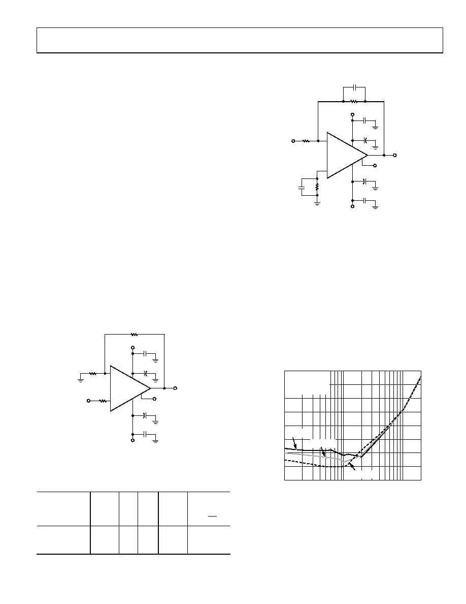
CIRCUIT CONSIDERATIONS
Balanced Input Impedances
Balanced input impedances can help to improve distortion
performance. When the amplifier transitions from PNP pair to
NPN pair operation, a change in both the magnitude and
direction of the input bias current occurs. When multiplied
times imbalanced input impedances, a change in offset can
result. The key to minimizing this distortion is to keep the input
impedances balanced on both inputs. Figure 59 shows the effect
of the imbalance and degradation in distortion performance for
a 50 Ω source impedance, with and without a 50 Ω balanced
feedback path.
FREQUENCY (MHz)
0.1
1
10
20
DISTORTION
(dB)
–100
–90
–80
–70
–60
–50
–40
–30
–20
G = +1
VOUT = 2V p-p
RL = 1kΩ
VS = +3V
RF = 24.9Ω
RF = 49.9Ω
RF = 0Ω
03327-A-058
Figure 59. SFDR vs. Frequency and Various RF
相关PDF资料 |
PDF描述 |
|---|---|
| AD8030ARZ-REEL7 | IC AMP GP R-R DUAL LP 8SOIC |
| 0034.5616.22 | FUSE 800MA 250V TLAG 5X20 SMD TR |
| ADA4930-2YCPZ-R2 | IC DIFF AMP 1.35GHZ 24-LFCSP |
| 0034.5617.22 | FUSE 1A 250V T-LAG 5X20 SMD T/R |
| KTR10EZPF1804 | RES 1.80M OHM 1/8W 1% 0805 SMD |
相关代理商/技术参数 |
参数描述 |
|---|---|
| AD8028 | 制造商:AD 制造商全称:Analog Devices 功能描述:Low Distortion, High Speed Rail-to-Rail Input/Output Amplifiers |
| AD8028AR | 制造商:Rochester Electronics LLC 功能描述:HIGH PERFORMANCE RRIO - Bulk 制造商:Analog Devices 功能描述:AMP LOW DISTORTION RRI/O SMD 8028 |
| AD8028AR-EBZ | 功能描述:BOARD EVAL FOR AD8028AR RoHS:是 类别:编程器,开发系统 >> 评估板 - 运算放大器 系列:- 产品培训模块:Lead (SnPb) Finish for COTS Obsolescence Mitigation Program 标准包装:1 系列:- |
| AD8028ARM | 制造商:Analog Devices 功能描述:OP Amp Dual GP R-R I/O ±6V/12V 10-Pin MSOP 制造商:Analog Devices 功能描述:AMP LOW DISTORTION RRI/O SMD 8028 |
| AD8028ARM-REEL | 制造商:Analog Devices 功能描述:OP Amp Dual GP R-R I/O ±6V/12V 10-Pin MSOP T/R |
发布紧急采购,3分钟左右您将得到回复。