- 您现在的位置:买卖IC网 > PDF目录11477 > AD8109ASTZ (Analog Devices Inc)IC VIDEO CROSSPOINT SWIT 80LQFP PDF资料下载
参数资料
| 型号: | AD8109ASTZ |
| 厂商: | Analog Devices Inc |
| 文件页数: | 18/33页 |
| 文件大小: | 0K |
| 描述: | IC VIDEO CROSSPOINT SWIT 80LQFP |
| 标准包装: | 1 |
| 功能: | 视频交叉点开关 |
| 电路: | 1 x 8:8 |
| 电压电源: | 双电源 |
| 电压 - 电源,单路/双路(±): | ±4.5 V ~ 5.5 V |
| 电流 - 电源: | 33mA |
| 工作温度: | -40°C ~ 85°C |
| 安装类型: | 表面贴装 |
| 封装/外壳: | 80-LQFP |
| 供应商设备封装: | 80-LQFP(12x12) |
| 包装: | 托盘 |
| 产品目录页面: | 801 (CN2011-ZH PDF) |
第1页第2页第3页第4页第5页第6页第7页第8页第9页第10页第11页第12页第13页第14页第15页第16页第17页当前第18页第19页第20页第21页第22页第23页第24页第25页第26页第27页第28页第29页第30页第31页第32页第33页
AD8108/AD8109
Rev. B | Page 24 of 32
PCB LAYOUT
Extreme care must be exercised to minimize additional
crosstalk generated by the system circuit board(s). The areas
that must be carefully detailed are grounding, shielding, signal
routing, and supply bypassing.
The packaging of the AD8108/AD8109 is designed to help keep
the crosstalk to a minimum. Each input is separated from each
other input by an analog ground pin. All of these AGNDs
should be directly connected to the ground plane of the circuit
board. These ground pins provide shielding, low impedance
return paths, and physical separation for the inputs. All of these
help to reduce crosstalk.
Each output is separated from its two neighboring outputs by an
analog ground pin in addition to an analog supply pin of one
polarity or the other. Each of these analog supply pins provides
power to the output stages of only the two nearest outputs.
These supply pins and analog grounds provide shielding,
physical separation, and a low impedance supply for the
outputs. Individual bypassing of each of these supply pins with a
0.01 F chip capacitor directly to the ground plane minimizes
high frequency output crosstalk via the mechanism of sharing
common impedances.
Each output also has an on-chip compensation capacitor
that is individually tied to the nearby analog ground pins
AGND00 through AGND07. This technique reduces crosstalk by
preventing the currents that flow in these paths from sharing a
common impedance on the IC and in the package pins. These
AGNDxx signals should all be directly connected to the ground
plane.
The input and output signals will have minimum crosstalk if
they are located between ground planes on layers above and
below, and separated by ground in between. Vias should be
located as close to the IC as possible to carry the inputs and
outputs to the inner layer. The only place the input and output
signals surface is at the input termination resistors and the
output series back-termination resistors. These signals should
also be separated, to the extent possible, as soon as they emerge
from the IC package.
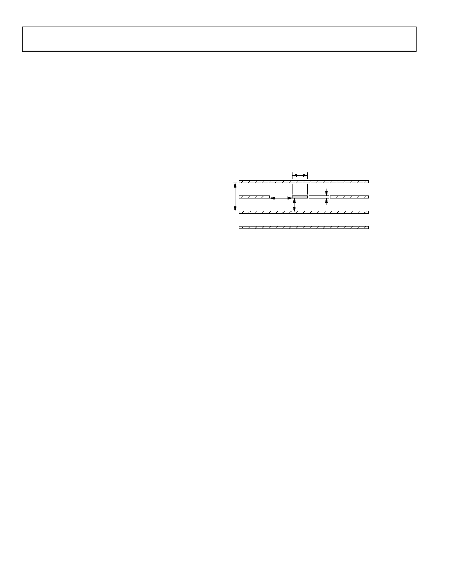
Optimized for video applications, all signal inputs and outputs
are terminated with 75 resistors. Stripline techniques are used
to achieve a characteristic impedance of 75 on the signal
input and output lines. Figure 52 shows a cross section of one of
the input or output tracks along with the arrangement of the
PCB layers. It should be noted that unused regions of the four
layers are filled up with ground planes. As a result, the input
and output traces, in addition to having controlled impedances,
are well shielded.
w = 0.008"
(0.2mm)
a = 0.008"
(0.2mm)
b = 0.024"
(0.6mm)
h = 0.011325"
(0.288mm)
t = 0.00135" (0.0343mm)
TOP LAYER
SIGNAL LAYER
POWER LAYER
BOTTOM LAYER
01068-
058
Figure 52. Cross Section of Input and Output Traces
The board has 16 BNC type connectors: eight inputs and eight
outputs. The connectors are arranged in two crescents around
the device. As can be seen from Figure 53, this results in all
eight input signal traces and all eight signal output traces having
the same length. This is useful in tests such as all-hostile
crosstalk where the phase relationship and delay between
signals needs to be maintained from input to output.
The three power supply pins AVCC, DVCC, and AVEE should
be connected to good quality, low noise, ±5 V supplies. Where
the same ±5 V power supplies are used for analog and digital,
separate cables should be run for the power supply to the
evaluation board’s analog and digital power supply pins.
As a general rule, each power supply pin (or group of adjacent
power supply pins) should be locally decoupled with a 0.01 F
capacitor. If there is a space constraint, it is more important to
decouple analog power supply pins before digital power supply
pins. A 0.1 F capacitor, located reasonably close to the pins,
can be used to decouple a number of power supply pins. Finally
a 10 F capacitor should be used to decouple power supplies as
they come onto the board.
相关PDF资料 |
PDF描述 |
|---|---|
| PIC16C55A-20/P | IC MCU OTP 512X12 28DIP |
| AD75019JPZ | IC CROSSPOINT SWIT 16X16 44PLCC |
| SY58024UMG | IC CROSSPOINT SWITCH DUAL 32MLF |
| SY58040UMY | IC CROSSPOINT SWITCH 4X4 44MLF |
| PIC16F726-E/ML | IC PIC MCU FLASH 8KX14 28-QFN |
相关代理商/技术参数 |
参数描述 |
|---|---|
| AD8109ASTZ | 制造商:Analog Devices 功能描述:Analog Crosspoint Switch IC |
| AD8109ASTZ2 | 制造商:AD 制造商全称:Analog Devices 功能描述:325 MHz, 8 ?? 8 Buffered Video Crosspoint Switches |
| AD8109-EB | 制造商:Analog Devices 功能描述:Evaluation Board For IC Video Cross PT 250MHz 8X8 制造商:Analog Devices 功能描述:VID CROSSPT 250MHZ 8X8 - Bulk 制造商:Rochester Electronics LLC 功能描述:AD8109 EVALUATION BOARD - Bulk |
| AD810ACHIPS | 制造商:Analog Devices 功能描述: |
| AD810AN | 功能描述:IC CURR-FDBK AMP VIDEO LP 8-DIP RoHS:否 类别:集成电路 (IC) >> 线性 - 放大器 - 视频放大器和频缓冲器 系列:- 标准包装:1,000 系列:- 应用:驱动器 输出类型:差分 电路数:3 -3db带宽:350MHz 转换速率:1000 V/µs 电流 - 电源:14.5mA 电流 - 输出 / 通道:60mA 电压 - 电源,单路/双路(±):5 V ~ 12 V,±2.5 V ~ 6 V 安装类型:表面贴装 封装/外壳:20-VFQFN 裸露焊盘 供应商设备封装:20-QFN 裸露焊盘(4x4) 包装:带卷 (TR) |
发布紧急采购,3分钟左右您将得到回复。