参数资料
| 型号: | AD8195ACPZ |
| 厂商: | Analog Devices Inc |
| 文件页数: | 5/20页 |
| 文件大小: | 0K |
| 描述: | IC BUFF HDMI/DVI W/EQUAL 40LFCSP |
| 标准包装: | 1 |
| 功能: | 开关 |
| 电路: | 1 x 1:1 |
| 电压电源: | 单电源 |
| 电压 - 电源,单路/双路(±): | 3 V ~ 3.6 V |
| 工作温度: | -40°C ~ 85°C |
| 安装类型: | 表面贴装 |
| 封装/外壳: | 40-VFQFN 裸露焊盘,CSP |
| 供应商设备封装: | 40-LFCSP-VQ(6x6) |
| 包装: | 托盘 |
Data Sheet
AD8195
Rev. B | Page 13 of 20
THEORY OF OPERATION
The primary function of the AD8195 is to buffer a single (HDMI
or DVI) link. The HDMI or DVI link consists of four differential,
high speed channels and three auxiliary single-ended, low speed
control signals. The high speed channels include a data-word clock
and three transition minimized differential signaling (TMDS)
data channels running at 10× the data-word clock frequency for
data rates up to 2.25 Gbps. The three low speed control signals
consist of the display data channel (DDC) bus (SDA and SCL)
and the consumer electronics control (CEC) line.
All four high speed TMDS channels are identical; that is, the
pixel clock can be run on any of the four TMDS channels.
Receive channel compensation is provided for the high speed
channels to support long input cables. The AD8195 also includes
selectable preemphasis for driving high loss output cables.
In the intended application, the AD8195 is placed between a
source and a sink, with long cable runs on the input and output.
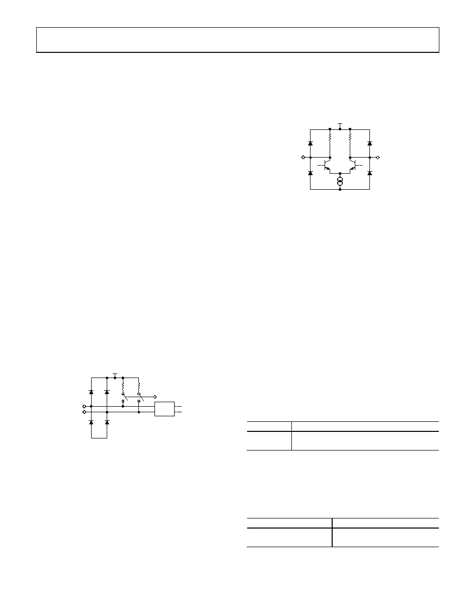
INPUT CHANNELS
Each high speed input differential pair terminates to the 3.3 V
VTTI power supply through a pair of single-ended 50 on-chip
resistors, as shown in Figure 30. When the transmitter of the
AD8195 is disabled by setting the TX_EN control pin, the input
termination resistors are also disabled to provide a high impedance
node at the TMDS inputs.
The input equalizer provides 12 dB of high frequency boost.
No specific cable length is suggested for this equalization level
because cable performance varies widely between manufacturers;
however, in general, the AD8195 does not degrade or over-
equalize input signals, even for short input cables. The AD8195
can equalize more than 20 meters of 24 AWG cable at 2.25 Gbps,
over reference cables that exhibit an insertion loss of 15 dB.
CABLE
EQ
50
IPx
TX_EN
INx
AVEE
VTTI
07049-
004
Figure 30. High Speed Input Simplified Schematic
OUTPUT CHANNELS
Each high speed output differential pair is terminated to the
3.3 V VTTO power supply through two single-ended 50
on-chip resistors (see Figure 31).
VTTO
50
OPx
ONx
AVEE
IOUT
07049-
005
Figure 31. High Speed Output Simplified Schematic
The output termination resistors of the AD8195 back terminate
the output TMDS transmission lines. These back terminations,
as `recommended in the HDMI specification, act to absorb
reflections from impedance discontinuities on the output traces,
improving the signal integrity of the output traces and adding
flexibility to how the output traces can be routed. For example,
interlayer vias can be used to route the AD8195 TMDS outputs
on multiple layers of the PCB without severely degrading the
quality of the output signal. Note that the arrangement of the
ESD structures cause current to flow into the TMDS outputs
when in the off state. The AD8195 outputs will not meet the
requirements of Test ID 7-3 (TMDS-VOFF) of the HDMI
Compliance Test Specification 1.3c. These outputs should only
interface to an internal system node and should not be interfaced
to an HDMI output connector.
The AD8195 has an external control pin, TX_EN, that disables
the transmitter, reducing power when the transmitter is not in
use. Additionally, when the transmitter is disabled, the input
termination resistors are also disabled to present a high impedance
state at the input and indicate to any connected HDMI sources
that the link through the AD8195 is inactive.
Table 7. Transmitter Enable Setting
TX_EN
Function
0
Tx/input termination disabled
1
Tx/input termination enabled
The AD8195 also includes two levels of programmable output
preemphasis, 0 dB and 6 dB. The output preemphasis level can
be manually configured by setting the PE_EN pin. No specific
cable length is suggested for use with either preemphasis setting,
as cable performance varies widely among manufacturers.
Table 8. Preemphasis Setting
PE_EN
PE Boost
0
0 dB
1
6 dB
相关PDF资料 |
PDF描述 |
|---|---|
| AD8196ACPZ | IC SWITCH DVI/HDMI 2:1 56-LFCSP |
| AD8197AASTZ | IC HDMI/DVI SWITCH 4:1 100LQFP |
| AD8197ASTZ-RL | IC SWITCH DVI/HDMI 4:1 100-LQFP |
| AD8197BASTZ-RL | IC SWITCH DVI/HDMI 4:1 100-LQFP |
| AD8303ARZ-REEL | IC DAC 12BIT SERIAL 14SOIC |
相关代理商/技术参数 |
参数描述 |
|---|---|
| AD8195ACPZ-R7 | 功能描述:IC BUFF HDMI/DVI W/EQUAL 40LFCSP RoHS:是 类别:集成电路 (IC) >> 接口 - 模拟开关,多路复用器,多路分解器 系列:- 标准包装:1,000 系列:- 功能:多路复用器 电路:1 x 4:1 导通状态电阻:- 电压电源:双电源 电压 - 电源,单路/双路(±):±5V 电流 - 电源:7mA 工作温度:-40°C ~ 85°C 安装类型:表面贴装 封装/外壳:16-SOIC(0.154",3.90mm 宽) 供应商设备封装:16-SOIC 包装:带卷 (TR) |
| AD8195-EVALZ | 制造商:Analog Devices 功能描述:EVALUATION BOARD - Boxed Product (Development Kits) |
| AD8195XCPZ | 功能描述:IC BUFF HDMI/DVI W/EQUAL 40LFCSP 制造商:analog devices inc. 系列:- 包装:托盘 零件状态:上次购买时间 类型:HDMI/DVI 缓冲器 应用:HDTV 安装类型:表面贴装 封装/外壳:40-VFQFN 裸露焊盘,CSP 供应商器件封装:40-LFCSP-VQ(6x6) 标准包装:1 |
| AD8196 | 制造商:AD 制造商全称:Analog Devices 功能描述:2:1 HDMI/DVI Switch with Equalization |
| AD8196ACPZ | 功能描述:IC SWITCH DVI/HDMI 2:1 56-LFCSP RoHS:是 类别:集成电路 (IC) >> 专用 IC 系列:- 产品培训模块:Lead (SnPb) Finish for COTS Obsolescence Mitigation Program 标准包装:1 系列:- 类型:调帧器 应用:数据传输 安装类型:表面贴装 封装/外壳:400-BBGA 供应商设备封装:400-PBGA(27x27) 包装:散装 |
发布紧急采购,3分钟左右您将得到回复。