参数资料
| 型号: | AD8195ACPZ |
| 厂商: | Analog Devices Inc |
| 文件页数: | 6/20页 |
| 文件大小: | 0K |
| 描述: | IC BUFF HDMI/DVI W/EQUAL 40LFCSP |
| 标准包装: | 1 |
| 功能: | 开关 |
| 电路: | 1 x 1:1 |
| 电压电源: | 单电源 |
| 电压 - 电源,单路/双路(±): | 3 V ~ 3.6 V |
| 工作温度: | -40°C ~ 85°C |
| 安装类型: | 表面贴装 |
| 封装/外壳: | 40-VFQFN 裸露焊盘,CSP |
| 供应商设备封装: | 40-LFCSP-VQ(6x6) |
| 包装: | 托盘 |
AD8195
Data Sheet
Rev. B | Page 14 of 20
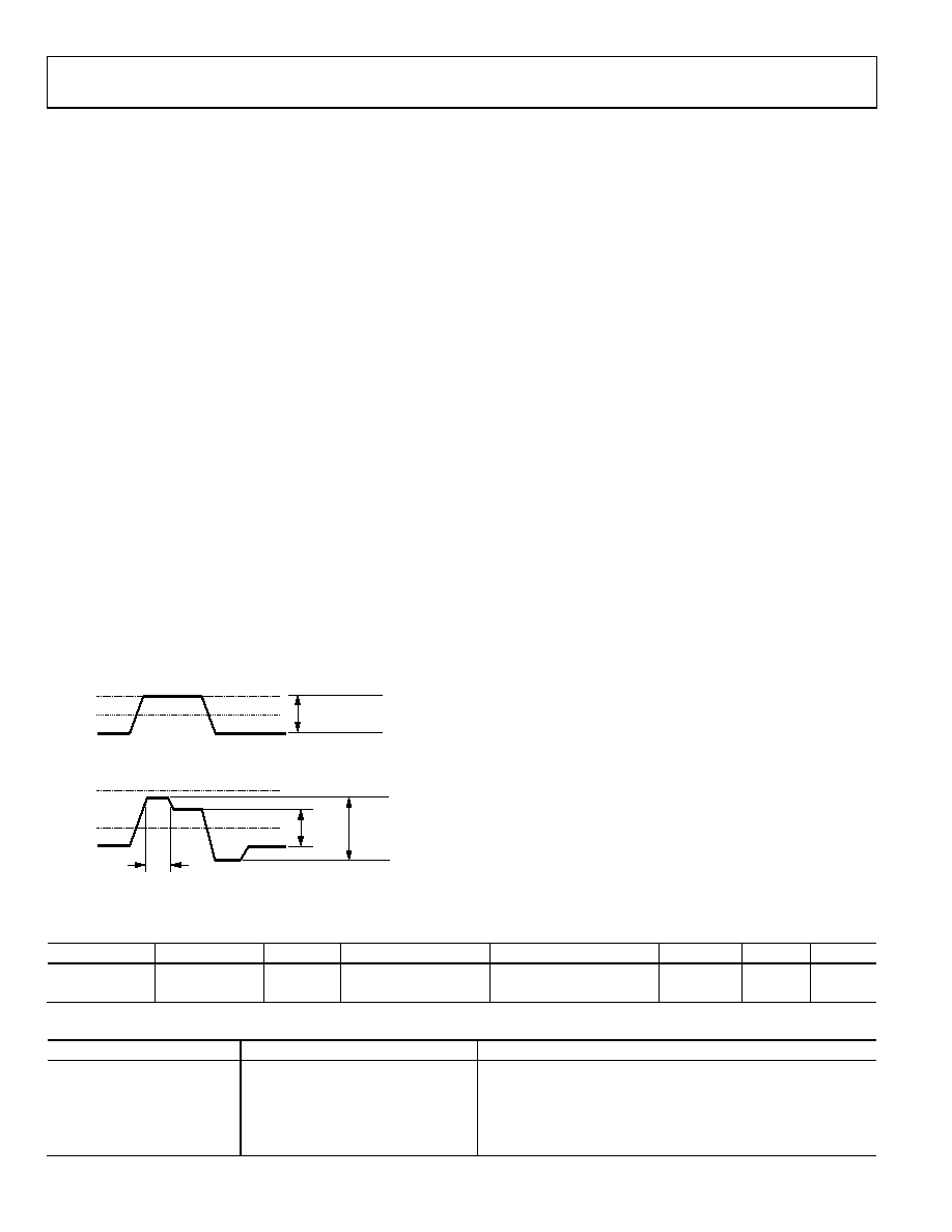
PREEMPHASIS
The preemphasized TMDS outputs precompensate the trans-
mitted signal to account for losses in systems with long cable
runs. These long cable runs selectively attenuate the high
frequency energy of the signal, leading to degraded transition
times and eye closure. Similar to a receive equalizer, the goal of
the preemphasis filter is to boost the high frequency energy in
the signal. However, unlike the receive equalizer, the preemphasis
filter is applied before the channel, thus predistorting the
transmitted signal to account for the loss of the channel. The
series connection of the preemphasis filter and the channel
results in a flatter frequency response than that of the channel,
thus leading to improved high frequency energy, improved
transition times, and improved eye opening on the far end of
the channel. Using a preemphasis filter to compensate for
channel losses allows for longer cable runs with or without a
receiver equalizer on the far end of the channel.
When there is no receive equalizer on the far end of the channel,
the preemphasis filter should allow longer cable runs than
would be acceptable with no preemphasis. When there is both a
preemphasis filter on the near end and a receive equalizer on
the far end of the channel, the allowable cable run should be
longer than either compensation could achieve alone. The pulse
response of a preemphasized waveform is shown in Figure 32.
The output voltage levels and symbol descriptions are listed in
Table 9 and Table 10, respectively. The preemphasis circuit is
designed to work up to 2.25 Gbps and does not perform
suitably at higher data rates.
VOCM
VH
VL
VOSE-BOOST
VTTO
VOSE-DC
<TBIT
VOCM
VTTO
VH
VL
VOSE-DC
PREEMPHASIS OFF
PREEMPHASIS ON
07049-
006
Figure 32. Preemphasis Pulse Response
AUXILIARY LINES
The auxiliary (low speed) lines provide buffering for the DDC
and CEC signals. The auxiliary lines are powered independently
from the TMDS link; therefore, their functionality can be
maintained even when the system is powered off. In an application,
these lines can be powered by connecting AMUXVCC to the
5 V supply provided from the video source through the input
HDMI connector.
DDC Buffers
The DDC buffers are 5 V tolerant bidirectional lines that can
carry extended display identification data (EDID), HDCP
encryption, and other information, depending on the specific
application. The DDC buffers are bidirectional and fully support
arbitration, clock synchronization, clock stretching, slave acknowl-
edgement, and other relevant features of a standard mode I2C bus.
The DDC buffers also have separate voltage references for the
input side and the output side, allowing the sink to use internal
bus voltages (3.3 V), alleviating the need for 5 V tolerant I/Os
for system ASICs. The logic level for the DDC_IN bus is set by
the voltage on VREF_IN, and the logic level for the DDC_OUT
bus is set by the voltage on VREF_OUT. For example, if the
DDC_IN bus is using 5 V I2C, the VREF_IN power supply pin
should be connected to a 5 V power supply. If the DDC_OUT
bus is using 3.3 V I2C, the VREF_OUT power supply pin should
be connected to a 3.3 V power supply.
CEC Buffer
The CEC buffer is a 3.3 V tolerant bidirectional buffer with
integrated pull-up resistors. This buffer enables full compliance
with all CEC specifications, including but not limited to input
capacitance, logic levels, transition times, and leakage (both with
the system power on and off). This allows the CEC functionality
to be implemented in a standard microcontroller that may not
have CEC compliant I/Os. The CEC buffer is powered from the
AMUXVCC supply.
Table 9. Output Voltage Levels
PE Setting
Boost (dB)
IT (mA)
VOSE-DC (mV p-p)
VOSE-BOOST (mV p-p)
VOCM (V)
VH (V)
VL (V)
0
20
500
3.050
3.3
2.8
1
6
40
500
1000
2.8
3.3
2.3
Table 10. Symbol Definitions
Symbol
Formula
Definition
VOSE-DC
IT|PE = 0 × 25
Single-ended output voltage swing after settling
VOSE-BOOST
IT × 25
Boosted single-ended output voltage swing
VOCM (DC-Coupled)
VTTO – IT/2 × 25
Common-mode voltage when the output is dc-coupled
VH
VOCM + VOSE-BOOST/2
High single-ended output voltage excursion
VL
VOCM VOSE-BOOST/2
Low single-ended output voltage excursion
相关PDF资料 |
PDF描述 |
|---|---|
| AD8196ACPZ | IC SWITCH DVI/HDMI 2:1 56-LFCSP |
| AD8197AASTZ | IC HDMI/DVI SWITCH 4:1 100LQFP |
| AD8197ASTZ-RL | IC SWITCH DVI/HDMI 4:1 100-LQFP |
| AD8197BASTZ-RL | IC SWITCH DVI/HDMI 4:1 100-LQFP |
| AD8303ARZ-REEL | IC DAC 12BIT SERIAL 14SOIC |
相关代理商/技术参数 |
参数描述 |
|---|---|
| AD8195ACPZ-R7 | 功能描述:IC BUFF HDMI/DVI W/EQUAL 40LFCSP RoHS:是 类别:集成电路 (IC) >> 接口 - 模拟开关,多路复用器,多路分解器 系列:- 标准包装:1,000 系列:- 功能:多路复用器 电路:1 x 4:1 导通状态电阻:- 电压电源:双电源 电压 - 电源,单路/双路(±):±5V 电流 - 电源:7mA 工作温度:-40°C ~ 85°C 安装类型:表面贴装 封装/外壳:16-SOIC(0.154",3.90mm 宽) 供应商设备封装:16-SOIC 包装:带卷 (TR) |
| AD8195-EVALZ | 制造商:Analog Devices 功能描述:EVALUATION BOARD - Boxed Product (Development Kits) |
| AD8195XCPZ | 功能描述:IC BUFF HDMI/DVI W/EQUAL 40LFCSP 制造商:analog devices inc. 系列:- 包装:托盘 零件状态:上次购买时间 类型:HDMI/DVI 缓冲器 应用:HDTV 安装类型:表面贴装 封装/外壳:40-VFQFN 裸露焊盘,CSP 供应商器件封装:40-LFCSP-VQ(6x6) 标准包装:1 |
| AD8196 | 制造商:AD 制造商全称:Analog Devices 功能描述:2:1 HDMI/DVI Switch with Equalization |
| AD8196ACPZ | 功能描述:IC SWITCH DVI/HDMI 2:1 56-LFCSP RoHS:是 类别:集成电路 (IC) >> 专用 IC 系列:- 产品培训模块:Lead (SnPb) Finish for COTS Obsolescence Mitigation Program 标准包装:1 系列:- 类型:调帧器 应用:数据传输 安装类型:表面贴装 封装/外壳:400-BBGA 供应商设备封装:400-PBGA(27x27) 包装:散装 |
发布紧急采购,3分钟左右您将得到回复。